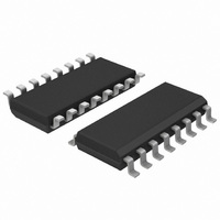
74LV165D,118 NXP Semiconductors, 74LV165D,118 Datasheet - Page 8

74LV165D,118
Manufacturer Part Number
74LV165D,118
Description
IC 8BIT SHIFT REGISTER 16SOIC
Manufacturer
NXP Semiconductors
Series
74LVr
Datasheet
1.74LV165N112.pdf
(14 pages)
Specifications of 74LV165D,118
Package / Case
16-SOIC (3.9mm Width)
Logic Type
Shift Register
Function
Parallel or Serial to Serial
Output Type
Differential
Number Of Elements
1
Number Of Bits Per Element
8
Voltage - Supply
1 V ~ 5.5 V
Operating Temperature
-40°C ~ 125°C
Mounting Type
Surface Mount
Counting Sequence
Serial/Parallel to Serial
Number Of Circuits
1
Logic Family
LV
Propagation Delay Time
18 ns
Supply Voltage (max)
5.5 V
Maximum Operating Temperature
+ 125 C
Minimum Operating Temperature
- 40 C
Mounting Style
SMD/SMT
Supply Voltage (min)
1 V
Lead Free Status / RoHS Status
Lead free / RoHS Compliant
Lead Free Status / RoHS Status
Lead free / RoHS Compliant, Lead free / RoHS Compliant
Other names
74LV165D-T
74LV165D-T
935156060118
74LV165D-T
935156060118
Philips Semiconductors
AC WAVEFORMS
V
V
V
output load.
Note to Figure 4
CE may change only from HIGH-to-LOW while CP is LOW. The
shaded areas indicate when the input is permitted to change for
predictable output performance.
1998 May 07
Figure 4. Set-up and hold times from the serial data input (D
enable input (CE) to the clock input (CP) and from the clock input
M
M
OL
the clock (CP) and the clock enable (CE) inputs, from the clock
8-bit parallel-in/serial-out shift register
CE may change only from HIGH-to-LOW while CP is LOW. The shaded
areas indicate when the input is permitted to change for predictable output
performance.
Figure 3. Data input (D
= 1.5 V at V
= 0.5
and V
D
S
CP, CE
CP, CE
INPUT
INPUT
INPUT
Q
Q
GND
GND
GND
OH
7
7
D
V
OUTPUT
OUTPUT
V
V
V
7
CC
I
I
I
INPUT
are the typical output voltage drop that occur with the
GND
CC
V
V
V
V
at V
OH
OH
(CP) to the clock enable input (CE).
OL
OL
V
I
CC
2.7 V.
see note
delays when PL is LOW.
V
M
t
su
2.7 V;
V
(L)
t
M
su
stable
t
t
n
V
PHL
PLH
) to output (Q
M
t
t
h
V
h
M
V
V
M
M
t
t
PHL
PLH
7
or Q
t
W
SV00592
t
su
7
) propagation
(H)
SV00595
t
h
S
) to
8
TEST CIRCUIT
Figure 5. Set-up and hold times from the data inputs (D
t
PLH/
GENERATOR
TEST
DEFINITIONS
R
C
R
D
PL INPUT
T
PULSE
L
L
t
n
PHL
= Load resistor
= Load capacitance includes jig and probe capacitiance
= Termination resistance should be equal to Z
INPUT
Figure 6. Load circuitry for switching times.
GND
GND
V
V
I
I
to the parallel load input (PL).
Test Circuit for Outputs
V
2.7–3.6V
V
l
< 2.7V
M
t
su
R
V
4.5 V
T
CC
t
V
H
M
D.U.T.
V
cc
2.7V
V
V
V
CC
CC
I
V
O
OUT
C
L
t
su
of pulse generators.
Product specification
50pF
74LV165
SV00593
t
H
SV00902
R
L
= 1k
n
)


