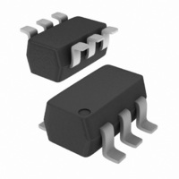
74AUP1T57GW,125 NXP Semiconductors, 74AUP1T57GW,125 Datasheet - Page 4

74AUP1T57GW,125
Manufacturer Part Number
74AUP1T57GW,125
Description
IC LP CONFIG GATE V-XLATR UMT6
Manufacturer
NXP Semiconductors
Series
74AUPr
Datasheet
1.74AUP1T57GF132.pdf
(20 pages)
Specifications of 74AUP1T57GW,125
Package / Case
SC-70-6, SC-88, SOT-363
Logic Function
Translator
Number Of Bits
2
Input Type
Voltage
Output Type
Voltage
Number Of Channels
2
Number Of Outputs/channel
1
Differential - Input:output
No/No
Propagation Delay (max)
3.8ns
Voltage - Supply
2.3 V ~ 3.6 V
Operating Temperature
-40°C ~ 125°C
Supply Voltage
2.3 V ~ 3.6 V
Logic Type
Voltage Level Translator
Logic Family
AUP
Input Bias Current (max)
50 mA
High Level Output Current
- 4 mA
Low Level Output Current
4 mA
Propagation Delay Time
8.2 ns @ 2.3 V to 2.7 V or 7 ns @ 3 V to 3.6 V
Supply Voltage (max)
3.6 V
Supply Voltage (min)
2.3 V
Maximum Operating Temperature
+ 125 C
Minimum Operating Temperature
- 40 C
Maximum Power Dissipation
250 mW
Mounting Style
SMD/SMT
Number Of Circuits
Configurable
Data Rate
-
Lead Free Status / RoHS Status
Lead free / RoHS Compliant
Data Rate
-
Lead Free Status / Rohs Status
Lead free / RoHS Compliant
Other names
74AUP1T57GW-G
74AUP1T57GW-G
935280464125
74AUP1T57GW-G
935280464125
NXP Semiconductors
Table 5.
74AUP1T57
Product data sheet
Logic function
2-input AND
2-input AND with both inputs inverted
2-input NAND with inverted input
2-input OR with inverted input
2-input NOR
2-input NOR with both inputs inverted
2-input XNOR
Inverter
Buffer
Fig 5.
Fig 7.
Fig 9.
2-input AND gate or 2-input NOR gate with
both inputs inverted
2-input NAND gate with input C inverted or
2-input OR gate with inverted A input
2-input XNOR gate
C
C
C
C
C
B
B
A
A
B
Function selection table
7.1 Logic configurations
Y
Y
Y
Y
Y
B
B
A
1
2
3
1
2
3
1
2
3
6
5
4
001aab584
6
5
4
001aab586
6
5
4
001aab588
All information provided in this document is subject to legal disclaimers.
C
Y
C
Y
C
Y
V
V
V
CC
CC
CC
Rev. 3 — 21 July 2010
Low-power configurable gate with voltage-level translator
Figure
see
see
see
see
see
see
see
see
see
Fig 6.
Fig 8.
Fig 10. Inverter
Figure 5
Figure 8
Figure 6
Figure 6
Figure 8
Figure 5
Figure 9
Figure 10
Figure 11
2-input NAND gate with input B inverted or
2-input OR gate with inverted C input
2-input NOR gate or 2-input AND gate with
both inputs inverted
C
C
C
C
B
B
A
A
A
and
and
7
7
Y
Y
Y
Y
Y
A
B
A
74AUP1T57
1
2
3
1
2
3
1
2
3
6
5
4
001aab589
© NXP B.V. 2010. All rights reserved.
6
5
4
6
5
4
001aab585
001aab587
Y
C
Y
C
Y
V
V
V
CC
CC
CC
4 of 20


