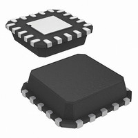
ISL3034EIRTZ Intersil, ISL3034EIRTZ Datasheet - Page 10

ISL3034EIRTZ
Manufacturer Part Number
ISL3034EIRTZ
Description
IC LEVEL TRANSLATOR 6CH 16-TQFN
Manufacturer
Intersil
Datasheet
1.ISL3034EIRTZ-T.pdf
(16 pages)
Specifications of ISL3034EIRTZ
Logic Function
Translator, Bidirectional
Number Of Bits
5
Input Type
Logic
Output Type
Logic
Data Rate
100Mbps
Number Of Channels
1
Number Of Outputs/channel
5
Differential - Input:output
No/No
Voltage - Supply
2.2 V ~ 3.6 V
Operating Temperature
-40°C ~ 85°C
Package / Case
16-WQFN Exposed Pad, 16-DQFN
Supply Voltage
2.2 V ~ 3.6 V
Lead Free Status / RoHS Status
Lead free / RoHS Compliant
Best-in-Class ESD Protection
All pins on these devices include class 3 (>12kV) Human
Body Model (HBM) ESD protection structures, but the input
and I/O pins incorporate advanced structures allowing
them to survive ESD events in excess of ±15kV HBM and
±15kV to IEC61000-4-2. The I/OV
vulnerable to ESD damage because they typically connect
to an exposed port on the exterior of the finished product.
Simply touching the port pins, or connecting a memory
card, can cause an ESD event that might destroy
unprotected ICs. These new ESD structures protect the
device whether or not it is powered up and without
degrading the level shifting performance. This built-in ESD
protection eliminates the need for board level protection
structures (e.g., transient suppression diodes) and the
associated, undesirable capacitive load they present. To
ensure the full benefit of the built-in ESD protection,
connect the IC’s GND pin directly to a low impedance GND
plane.
IEC61000-4-2 Testing
The IEC61000 test method applies to finished equipment,
rather than to an individual IC. Therefore, the pins most likely
to suffer an ESD event are those that are exposed to the
outside world (typically I/OV
applications) but the ISL3034E, ISL3035E, and ISL3036E
feature IEC61000 ESD protection on all logic and I/O pins
(both I/OV
and MM methods which only test each pin-to-pin
combination without applying power, IEC61000 testing is
also performed with the IC in its typical application
Typical Performance Curves
FIGURE 7. V
2.5
2.0
1.5
1.0
0.5
0
2.2
L
and I/OV
2.4
L
SUPPLY CURRENT vs V
SWITCHING 4 I/OV
V
SWITCHING 1 I/OV
CC
CC
2.6
SWITCHING 6 I/OV
, as well as CLK pins). Unlike HBM
SUPPLY VOLTAGE (V)
CC
2.8
10
pins in memory card
CC
L
3.0
L
INPUTS
INPUT
pins are particularly
L
CC
INPUTS
SUPPLY VOLTAGE
3.2
ISL3034E, ISL3035E, ISL3036E
V
T
A
CC
= +25°C; Unless Otherwise Specified.
V
= 3.3V, V
3.4
L
= 1.8V
3.6
L
= 1.8V, C
L
= 15pF, R
configuration (power applied). The IEC61000 standard’s
lower current limiting resistor coupled with the larger charge
storage capacitor yields a test that is much more severe than
the HBM test. The extra ESD protection built into these
devices’ pins allows the design of equipment meeting level 4
criteria without the need for additional board level protection.
AIR-GAP DISCHARGE TEST METHOD
For this test method, a charged probe tip moves toward the
IC pin until the voltage arcs to it. The current waveform
delivered to the IC pin depends on approach speed,
humidity, temperature, etc., so it is difficult to obtain
repeatable results. All the EN, CLK, and I/O pins withstand
±15kV air-gap discharges, relative to GND.
CONTACT DISCHARGE TEST METHOD
During the contact discharge test, the probe contacts the
tested pin before the probe tip is energized, thereby
eliminating the variables associated with the air-gap
discharge. The result is a more repeatable and predictable
test, but equipment limits prevent testing devices at voltages
higher than ±9kV. Devices in this family survive ±9kV contact
discharges (relative to the GND pin) on the EN, CLK, and I/O
pins.
Layout and Decoupling Considerations
These level translators’ high data rates and fast signal
transitions require that the accelerators have high transient
currents. Thus, short, low inductance supply traces and
decoupling within 1/8th inch of the IC are imperative with
very low impedance GND return paths.
FIGURE 8. V
25
20
15
10
5
0
1.3
SOURCE
SWITCHING 1 I/OV
V
SWITCHING 6 I/OV
CC
1.5
= 3.6V
L
SUPPLY CURRENT vs V
= 150Ω, Data Rate = 100Mbps, push-pull driver,
1.7
V
1.9
L
CC
CC
SUPPLY VOLTAGE (V)
INPUT
INPUTS
2.1
SWITCHING 4 I/OV
2.3
2.5
L
SUPPLY VOLTAGE
2.7
CC
2.9
March 31, 2009
INPUTS
FN6492.0
3.1
3.2


