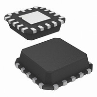
ISL3035EIRTZ-T Intersil, ISL3035EIRTZ-T Datasheet - Page 8

ISL3035EIRTZ-T
Manufacturer Part Number
ISL3035EIRTZ-T
Description
IC LEVEL TRANSLATOR 6CH 16-TQFN
Manufacturer
Intersil
Datasheet
1.ISL3034EIRTZ-T.pdf
(16 pages)
Specifications of ISL3035EIRTZ-T
Logic Function
Translator, Bidirectional
Number Of Bits
5
Input Type
Logic
Output Type
Logic
Data Rate
100Mbps
Number Of Channels
1
Number Of Outputs/channel
5
Differential - Input:output
No/No
Voltage - Supply
2.2 V ~ 3.6 V
Operating Temperature
-40°C ~ 85°C
Package / Case
16-WQFN Exposed Pad, 16-DQFN
Supply Voltage
2.2 V ~ 3.6 V
Lead Free Status / RoHS Status
Lead free / RoHS Compliant
Application Information
Overview
The ISL3034E, ISL3035E, ISL3036E are 100Mbps,
bi-directional voltage level translating ICs for multi-supply
voltage systems. These products shift lower voltage levels
on one interface side (supplied by V
level on the other interface side (supplied by V
versa. V
of the I/OV
These ICs feature bit-by-bit auto-direction sensing to
increase flexibility, and to eliminate the need for direction
control pins. On chip pull-up current sources in the active
mode, and pull-up resistors in SHDN mode, eliminate the
need for most external bus resistors. Drivers interfacing with
these level translators may be open-drain or push-pull types,
and all three versions may also be used for unidirectional
level shifting.
The three versions share the same architecture, but the
ISL3034E is a general purpose 6-Channel version, while the
6-Channel ISL3035E specifically targets SD Card and other
memory card applications. The 4-channel ISL3036 targets
nibble and byte based applications, as well as 4-wire SPI
interfaces. Power supply ranges allow level shifting between
1.5V, 1.8V, and 2.5V powered devices on the V
2.5V, and 3.3V devices on the V
Principles of Operation
When enabled, these level shifters detect transitions on an
I/O pin, and drive the appropriate logic level on the
corresponding I/O pin on the other “side”. If the transition
was low-to-high, the channel shifts the voltage up to V
transitions on an I/OV
an I/OV
side. The ISL3035E enables whenever V
while the ISL3034E and ISL3036E enable if EN = 1 AND
V
Upon detecting a transition on either I/O pin, that channel’s
accelerator circuitry actively drives the opposite side’s
(output) pin to GND or the output’s supply rail, and then turns
off. Weak hold circuitry then maintains the logic state until
the input is 3-stated, or until another active transition occurs
on either I/O pin for that channel. Figure 5 shows the
simplified block diagram of one level shifting channel. The
accelerator circuitry comprises high and low threshold
detectors, one shots with level shifters and large output
drivers. A transition on one of the I/OV
momentarily defines that pin as an input. When the high or
low threshold is crossed, a one-shot fires either the PMOS or
NMOS driver, respectively, on the opposite side (effectively
the output). These drivers are large enough to quickly drive
the output node to its respective supply or to GND. Note that
this transition on the “output” trips the transition detector on
that pin, firing its accelerator, which feeds back to the “input”
to help reinforce slow transitions, such as those from an
CC
> V
CC
OH
L
+ 200mV.
CC
pin), and then drives the shifted level on the other
of the I/OV
pins tracks the V
L
L
pin) or down to V
pins tracks the V
8
CC
CC
supply.
side.
L
) to a higher voltage
L
or I/OV
L
L
CC
supply, while V
(for transitions on
ISL3034E, ISL3035E, ISL3036E
> V
CC
L
CC
L
side to
), or vice
+ 200mV,
pins
CC
(for
OH
open-drain type driver. Once the one-shot - and thus the
accelerator - times out (approximately 3ns to 4ns), the large
output drivers tri-state and the pins are weakly held in the
last state by the small NMOS transistor between I/OV
I/OV
high). In this static state, the I/O pins are easily overdriven by
the next transition from an external driver. Having large
pull-up and pull-down devices in the accelerator (vs just an
active pull-up) nearly eliminates the concern about the
external driver’s output impedance, and that impedance’s
effect on V
The weak pull-up current sources on each I/O pin and the
NMOS pass transistors, remain ON whenever the IC is
enabled. If a channel’s external driver tri-states, the weak
pull-up currents either keep the I/O pins high, or if the last
state was a low the current sources pull the I/O pins high. In
the latter case, each channel’s accelerators will once again
fire when either the I/OV
accelerator’s high threshold level.
Auto Direction Sensing
Each level translator channel independently and
automatically determines the direction of data transfer
without any external control signals. As described earlier, a
transition on either of the channel’s I/O pins momentarily
defines that pin as an input, which then translates and drives
that input signal to the channel’s corresponding pin on the
other port (now the output). After a brief period of active
driving, both I/O pins return to their weak “hold” mode, where
the next transition on either I/O pin determines the direction
for the next transfer.
Auto sensing saves valuable processor GPIO pins (three
[CLK, CMD, DAT] for SD Card applications, or six for the
general purpose hex case), and simplifies the software
associated with the peripheral interface.
Using Open Drain Drivers
These level translators’ accelerator based architecture
works equally well when driven by push-pull or open drain
type drivers (e.g., for the CMD line initialization in MMC
I/OV
CC
FIGURE 5. ONE CHANNEL SIMPLIFIED SCHEMATIC
L
(for a low) or by the small current sources (for a
OL
V
L
, fall times and data rate.
# ONE-SHOT AND LEVEL SHIFTER
V
L
HIGH V
LOW V
DETECT
DETECT
#
#
L
TH
TH
or the I/OV
EN
HIGH V
LOW V
DETECT
DETECT
#
#
CC
TH
TH
voltage crosses the
V
CC
V
CC
March 31, 2009
I/OV
L
FN6492.0
and
CC


