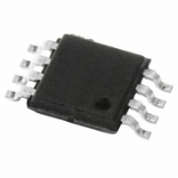
M95512-RDW6P STMicroelectronics, M95512-RDW6P Datasheet - Page 12

M95512-RDW6P
Manufacturer Part Number
M95512-RDW6P
Description
IC EEPROM 512KBIT 2MHZ 8TSSOP
Manufacturer
STMicroelectronics
Datasheet
1.M95512-RDW6TP.pdf
(48 pages)
Specifications of M95512-RDW6P
Format - Memory
EEPROMs - Serial
Memory Type
EEPROM
Memory Size
512K (64K x 8)
Speed
2MHz
Interface
SPI, 3-Wire Serial
Voltage - Supply
1.8 V ~ 5.5 V
Operating Temperature
-40°C ~ 85°C
Package / Case
8-TSSOP
Lead Free Status / RoHS Status
Lead free / RoHS Compliant
Available stocks
Company
Part Number
Manufacturer
Quantity
Price
Operating features
4
4.1
4.1.1
4.1.2
4.1.3
12/48
Operating features
Supply voltage (V
Operating supply voltage V
Prior to selecting the memory and issuing instructions to it, a valid and stable V
within the specified [V
Table
instruction and, for a Write instruction, until the completion of the internal write cycle (t
order to secure a stable DC supply voltage, it is recommended to decouple the V
a suitable capacitor (usually of the order of 10 nF to 100 nF) close to the V
pins.
Device reset
In order to prevent inadvertent Write operations during power-up, a power-on-reset (POR)
circuit is included. At power-up, the device does not respond to any instruction until V
reached the POR threshold voltage (this threshold is lower than the minimum V
voltage defined in
When V
●
●
●
When V
Power mode, however, the device must not be accessed until V
stable V
Table
Power-up conditions
When the power supply is turned on, V
time, the Chip Select (S) line is not allowed to float but should follow the V
therefore recommended to connect the S line to V
Figure
In addition, the Chip Select (S) input offers a built-in safety feature, as the S input is edge
sensitive as well as level sensitive: after power-up, the device does not become selected
until a falling edge has first been detected on Chip Select (S). This ensures that Chip Select
(S) must have been high, prior to going low to start the first operation.
The V
defined in
in the Standby Power mode
deselected (note that when the device is deselected it is necessary to apply a falling
edge on Chip Select (S) prior to issuing any new instruction, otherwise the instruction is
not executed)
Status register values:
–
–
–
10.). This voltage must remain stable and valid until the end of the transmission of the
10.
CC
4).
CC
CC
CC
voltage has to rise continuously from 0 V up to the minimum V
the Write Enable Latch (WEL) bit is reset to 0
the Write In Progress (WIP) bit is reset to 0
the SRWD, BP1 and BP0 bits remain unchanged (non-volatile bits).
Table 8
passes over the POR threshold, the device is reset and in the following state:
passes over the POR threshold, the device is reset and enters the Standby
voltage within the specified [V
Table 8
and
CC
Table 10
(min), V
and
CC
Doc ID 11124 Rev 14
)
Table
and the rise time must not vary faster than 1 V/µs.
CC
CC
(max)] range must be applied (see
10).
CC
CC
rises continuously from V
(min), V
CC
CC
via a suitable pull-up resistor (see
(max)] range defined in
M95512-DR, M95512-W, M95512-R
CC
reaches a valid and
SS
Table 8
to V
CC
CC
operating voltage
CC
CC
voltage. It is
/V
. During this
and
Table 8
CC
CC
SS
CC
operating
package
voltage
line with
CC
W
and
). In
has


