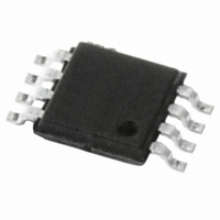
M95512-RDW6P STMicroelectronics, M95512-RDW6P Datasheet - Page 30

M95512-RDW6P
Manufacturer Part Number
M95512-RDW6P
Description
IC EEPROM 512KBIT 2MHZ 8TSSOP
Manufacturer
STMicroelectronics
Datasheet
1.M95512-RDW6TP.pdf
(48 pages)
Specifications of M95512-RDW6P
Format - Memory
EEPROMs - Serial
Memory Type
EEPROM
Memory Size
512K (64K x 8)
Speed
2MHz
Interface
SPI, 3-Wire Serial
Voltage - Supply
1.8 V ~ 5.5 V
Operating Temperature
-40°C ~ 85°C
Package / Case
8-TSSOP
Lead Free Status / RoHS Status
Lead free / RoHS Compliant
Available stocks
Company
Part Number
Manufacturer
Quantity
Price
ECC (error correction code) and write cycling
7
8
8.1
8.2
30/48
ECC (error correction code) and write cycling
The M95512-W, M95512-R and M95512-DR devices offer an ECC (error correction code)
logic which compares each 4-byte word with its associated 6 EEPROM bits of ECC. As a
result, if a single bit out of 4 bytes of data happens to be erroneous during a Read operation,
the ECC detects it and replaces it by the correct value. The read reliability is therefore much
improved by the use of this feature.
Note however that even if a single byte has to be written, 4 bytes are internally modified
(plus the ECC bits), that is, the addressed byte is cycled together with the other three bytes
making up the word. It is therefore recommended to write data by word (4 bytes) at address
4*N (where N is an integer) in order to benefit from the larger amount of Write cycles.
The M95512-W, M95512-R and M95512-DR devices are qualified at 1 million (1 000 000)
Write cycles, using a cycling routine that writes to the device by multiples of 4-byte packets.
Power-up and delivery state
Power-up state
After power-up, the device is in the following state:
●
●
●
●
●
The SRWD, BP1 and BP0 bits of the Status Register are unchanged from the previous
power-down (they are non-volatile bits).
Initial delivery state
The device is delivered with the memory array set at all 1s (FFh). The Status Register Write
Disable (SRWD) and Block Protect (BP1 and BP0) bits are initialized to 0.
Standby Power mode
Deselected (after Power-up, a falling edge is required on Chip Select (S) before any
instructions can be started).
Not in the Hold Condition
Write Enable Latch (WEL) is reset to 0
Write In Progress (WIP) is reset to 0
Doc ID 11124 Rev 14
M95512-DR, M95512-W, M95512-R


