AT45DB041B-RI Atmel, AT45DB041B-RI Datasheet - Page 11
AT45DB041B-RI
Manufacturer Part Number
AT45DB041B-RI
Description
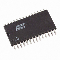
IC FLASH 4MBIT 20MHZ 28SOIC
Manufacturer
Atmel
Datasheet
1.AT45DB041B-CC.pdf
(35 pages)
Specifications of AT45DB041B-RI
Format - Memory
FLASH
Memory Type
DataFLASH
Memory Size
4M (2048 pages x 264 bytes)
Speed
20MHz
Interface
SPI, 3-Wire Serial
Voltage - Supply
2.7 V ~ 3.6 V
Operating Temperature
-40°C ~ 85°C
Package / Case
28-SOIC (7.5mm Width)
Lead Free Status / RoHS Status
Contains lead / RoHS non-compliant
Available stocks
Company
Part Number
Manufacturer
Quantity
Price
Company:

Part Number:
AT45DB041B-RI
Manufacturer:
ST
Quantity:
28
Part Number:
AT45DB041B-RI
Manufacturer:
ATMEL/爱特梅尔
Quantity:
20 000


5.5
5.5.1
5.5.2
5.5.3
5.5.4
5.5.5
5.5.6
5.5.7
3443D–DFLSH–2/08
Pin Descriptions
Serial Input (SI)
Serial Output (SO)
Serial Clock (SCK)
Chip Select (CS)
Write Protect (WP)
RESET
READY/BUSY
The SI pin is an input-only pin and is used to shift data into the device. The SI pin is used for all
data input including opcodes and address sequences.
The SO pin is an output-only pin and is used to shift data out from the device.
The SCK pin is an input-only pin and is used to control the flow of data to and from the
DataFlash. Data is always clocked into the device on the rising edge of SCK and clocked out of
the device on the falling edge of SCK.
The DataFlash is selected when the CS pin is low. When the device is not selected, data will not
be accepted on the SI pin, and the SO pin will remain in a high-impedance state. A high-to-low
transition on the CS pin is required to start an operation, and a low-to-high transition on the CS
pin is required to end an operation.
If the WP pin is held low, the first 256 pages of the main memory cannot be reprogrammed. The
only way to reprogram the first 256 pages is to first drive the protect pin high and then use the
program commands previously mentioned. If this pin and feature are not utilized it is recom-
mended that the WP pin be driven high externally.
A low state on the reset pin (RESET) will terminate the operation in progress and reset the inter-
nal state machine to an idle state. The device will remain in the reset condition as long as a low
level is present on the RESET pin. Normal operation can resume once the RESET pin is brought
back to a high level.
The device incorporates an internal power-on reset circuit, so there are no restrictions on the
RESET pin during power-on sequences. If this pin and feature are not utilized it is recommended
that the RESET pin be driven high externally.
This open drain output pin will be driven low when the device is busy in an internally self-timed
operation. This pin, which is normally in a high state (through a 1 kΩ external pull-up resistor),
will be pulled low during programming operations, compare operations, and during page-to-
buffer transfers.
The busy status indicates that the Flash memory array and one of the buffers cannot be
accessed; read and write operations to the other buffer can still be performed.
AT45DB041B
11
Related parts for AT45DB041B-RI
Image
Part Number
Description
Manufacturer
Datasheet
Request
R

Part Number:
Description:
DEV KIT FOR AVR/AVR32
Manufacturer:
Atmel
Datasheet:

Part Number:
Description:
INTERVAL AND WIPE/WASH WIPER CONTROL IC WITH DELAY
Manufacturer:
ATMEL Corporation
Datasheet:
Part Number:
Description:
Low-Voltage Voice-Switched IC for Hands-Free Operation
Manufacturer:
ATMEL Corporation
Datasheet:
Part Number:
Description:
MONOLITHIC INTEGRATED FEATUREPHONE CIRCUIT
Manufacturer:
ATMEL Corporation
Datasheet:
Part Number:
Description:
AM-FM Receiver IC U4255BM-M
Manufacturer:
ATMEL Corporation
Datasheet:
Part Number:
Description:
Monolithic Integrated Feature Phone Circuit
Manufacturer:
ATMEL Corporation
Datasheet:
Part Number:
Description:
Multistandard Video-IF and Quasi Parallel Sound Processing
Manufacturer:
ATMEL Corporation
Datasheet:
Part Number:
Description:
High-performance EE PLD
Manufacturer:
ATMEL Corporation
Datasheet:
Part Number:
Description:
8-bit Flash Microcontroller
Manufacturer:
ATMEL Corporation
Datasheet:
Part Number:
Description:
2-Wire Serial EEPROM
Manufacturer:
ATMEL Corporation
Datasheet: