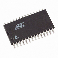
AT45DB041B-RI Atmel, AT45DB041B-RI Datasheet - Page 4

AT45DB041B-RI
Manufacturer Part Number
AT45DB041B-RI
Description
IC FLASH 4MBIT 20MHZ 28SOIC
Manufacturer
Atmel
Datasheet
1.AT45DB041B-CC.pdf
(35 pages)
Specifications of AT45DB041B-RI
Format - Memory
FLASH
Memory Type
DataFLASH
Memory Size
4M (2048 pages x 264 bytes)
Speed
20MHz
Interface
SPI, 3-Wire Serial
Voltage - Supply
2.7 V ~ 3.6 V
Operating Temperature
-40°C ~ 85°C
Package / Case
28-SOIC (7.5mm Width)
Lead Free Status / RoHS Status
Contains lead / RoHS non-compliant
Available stocks
Company
Part Number
Manufacturer
Quantity
Price
Company:
Part Number:
AT45DB041B-RI
Manufacturer:
ST
Quantity:
28
Part Number:
AT45DB041B-RI
Manufacturer:
ATMEL/爱特梅尔
Quantity:
20 000
5. Device Operation
5.1
5.1.1
4
Read Commands
AT45DB041B
Continuous Array Read
The device operation is controlled by instructions from the host processor. The list of instructions
and their associated opcodes are contained in Tables 1 through 4. A valid instruction starts with
the falling edge of CS followed by the appropriate 8-bit opcode and the desired buffer or main
memory address location. While the CS pin is low, toggling the SCK pin controls the loading of
the opcode and the desired buffer or main memory address location through the SI (serial input)
pin. All instructions, addresses and data are transferred with the most significant bit (MSB) first.
Buffer addressing is referenced in the datasheet using the terminology BFA8 - BFA0 to denote
the nine address bits required to designate a byte address within a buffer. Main memory
addressing is referenced using the terminology PA10 - PA0 and BA8 - BA0 where PA10 - PA0
denotes the 11 address bits required to designate a page address and BA8 - BA0 denotes the
nine address bits required to designate a byte address within the page.
By specifying the appropriate opcode, data can be read from the main memory or from either
one of the two data buffers. The DataFlash supports two categories of read modes in relation to
the SCK signal. The differences between the modes are in respect to the inactive state of the
SCK signal as well as which clock cycle data will begin to be output. The two categories, which
are comprised of four modes total, are defined as Inactive Clock Polarity Low or Inactive Clock
Polarity High and SPI Mode 0 or SPI Mode 3. A separate opcode (refer to
for a complete list) is used to select which category will be used for reading. Please refer to the
“Detailed Bit-level Read Timing” diagrams in this datasheet for details on the clock cycle
sequences for each mode.
By supplying an initial starting address for the main memory array, the Continuous Array Read
command can be utilized to sequentially read a continuous stream of data from the device by
simply providing a clock signal; no additional addressing information or control signals need to
be provided. The DataFlash incorporates an internal address counter that will automatically
increment on every clock cycle, allowing one continuous read operation without the need of
additional address sequences. To perform a continuous read, an opcode of 68H or E8H must be
clocked into the device followed by 24 address bits and 32 don’t care bits. The first four bits of
the 24-bit address sequence are reserved for upward and downward compatibility to larger and
smaller density devices (see Notes under “Command Sequence for Read/Write Operations” dia-
gram). The next 11 address bits (PA10 - PA0) specify which page of the main memory array to
read, and the last nine bits (BA8 - BA0) of the 24-bit address sequence specify the starting byte
address within the page. The 32 don’t care bits that follow the 24 address bits are needed to ini-
tialize the read operation. Following the 32 don’t care bits, additional clock pulses on the SCK
pin will result in serial data being output on the SO (serial output) pin.
The CS pin must remain low during the loading of the opcode, the address bits, the don’t care
bits, and the reading of data. When the end of a page in main memory is reached during a Con-
tinuous Array Read, the device will continue reading at the beginning of the next page with no
delays incurred during the page boundary crossover (the crossover from the end of one page to
the beginning of the next page). When the last bit in the main memory array has been read, the
device will continue reading back at the beginning of the first page of memory. As with crossing
over page boundaries, no delays will be incurred when wrapping around from the end of the
array to the beginning of the array.
Table 5-3 on page 10
3443D–DFLSH–2/08


