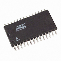
AT45DB041B-RI Atmel, AT45DB041B-RI Datasheet - Page 9

AT45DB041B-RI
Manufacturer Part Number
AT45DB041B-RI
Description
IC FLASH 4MBIT 20MHZ 28SOIC
Manufacturer
Atmel
Datasheet
1.AT45DB041B-CC.pdf
(35 pages)
Specifications of AT45DB041B-RI
Format - Memory
FLASH
Memory Type
DataFLASH
Memory Size
4M (2048 pages x 264 bytes)
Speed
20MHz
Interface
SPI, 3-Wire Serial
Voltage - Supply
2.7 V ~ 3.6 V
Operating Temperature
-40°C ~ 85°C
Package / Case
28-SOIC (7.5mm Width)
Lead Free Status / RoHS Status
Contains lead / RoHS non-compliant
Available stocks
Company
Part Number
Manufacturer
Quantity
Price
Company:
Part Number:
AT45DB041B-RI
Manufacturer:
ST
Quantity:
28
Part Number:
AT45DB041B-RI
Manufacturer:
ATMEL/爱特梅尔
Quantity:
20 000
5.4
3443D–DFLSH–2/08
Operation Mode Summary
take place in a maximum time of t
part is busy.
If a sector is programmed or reprogrammed sequentially page-by-page, then the programming
algorithm shown in
page or several pages are programmed randomly in a sector, then the programming algorithm
shown in
updated/rewritten at least once within every 10,000 cumulative page erase/program operations
in that sector.
The modes described can be separated into two groups – modes which make use of the Flash
memory array (Group A) and modes which do not make use of the Flash memory array (Group
B).
Group A modes consist of:
Group B modes consist of:
If a Group A mode is in progress (not fully completed) then another mode in Group A should not
be started. However, during this time in which a Group A mode is in progress, modes in Group B
can be started.
This gives the Serial DataFlash the ability to virtually accommodate a continuous data stream.
While data is being programmed into main memory from buffer 1, data can be loaded into buffer
2 (or vice versa). See application note AN-4 (“Using Atmel’s Serial DataFlash”) for more details.
1. Main Memory Page Read
2. Main Memory Page to Buffer 1 (or 2) Transfer
3. Main Memory Page to Buffer 1 (or 2) Compare
4. Buffer 1 (or 2) to Main Memory Page Program with Built-in Erase
5. Buffer 1 (or 2) to Main Memory Page Program without Built-in Erase
6. Page Erase
7. Block Erase
8. Main Memory Page Program through Buffer
9. Auto Page Rewrite
1. Buffer 1 (or 2) Read
2. Buffer 1 (or 2) Write
3. Status Register Read
Figure 17-2
Figure 17-1
on
page 28
on
EP
page 27
. During this time, the status register will indicate that the
is recommended. Each page within a sector must be
is recommended. Otherwise, if multiple bytes in a
AT45DB041B
9


