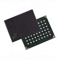
MT45W4MW16BCGB-701 WT Micron Technology Inc, MT45W4MW16BCGB-701 WT Datasheet - Page 31

MT45W4MW16BCGB-701 WT
Manufacturer Part Number
MT45W4MW16BCGB-701 WT
Description
IC PSRAM 64MBIT 70NS 54VFBGA
Manufacturer
Micron Technology Inc
Datasheet
1.MT45W4MW16BCGB-701_IT.pdf
(69 pages)
Specifications of MT45W4MW16BCGB-701 WT
Format - Memory
RAM
Memory Type
PSRAM (Page)
Memory Size
64M (4M x 16)
Speed
70ns
Interface
Parallel
Voltage - Supply
1.7 V ~ 1.95 V
Operating Temperature
-30°C ~ 85°C
Package / Case
54-VFBGA
Operating Temperature (max)
85C
Mounting
Surface Mount
Operating Temperature Classification
Commercial
Lead Free Status / RoHS Status
Lead free / RoHS Compliant
Refresh Configuration Register
Partial-Array Refresh (RCR[2:0]) Default = Full Array Refresh
Figure 24:
PDF: 09005aef8247bd51/Source: 09005aef8247bd83
64mb_burst_cr1_5_p25z_133mhz__2.fm - Rev. F 9/07 EN
RCR[19]
0
1
0
RCR[7]
0
1
RCR[18]
All must be set to “0”
0
0
1
Refresh Configuration Register Mapping
Page mode disabled (default)
Page mode enable
Page Mode Enable/Disable
Reserved
Register Select
Select RCR
Select BCR
Select DIDR
A[21:20] A[19:18]
21–20
Register
Select
19–18
All must be set to “0”
The refresh configuration register (RCR) defines how the CellularRAM device performs
its transparent self refresh. Altering the refresh parameters can dramatically reduce
current consumption during standby mode. Page mode control is also embedded into
the RCR. Figure 24 describes the control bits used in the RCR. At power-up, the RCR is set
to 0010h.
The RCR is accessed with CRE HIGH and A[19:18] = 00b or through the register access
software sequence with DQ = 0000h on the third cycle (see “Registers” on page 18).
The PAR bits restrict refresh operation to a portion of the total memory array. This
feature allows the device to reduce standby current by refreshing only that part of the
memory array required by the host system. The refresh options are full array, one-half
array, one-quarter array, one-eighth array, or none of the array. The mapping of these
partitions can start either at the beginning or the end of the address map (see Table 8 on
page 32).
Reserved
17–8
64Mb: 4 Meg x 16 Async/Page/Burst CellularRAM 1.5 Memory
A[17:8]
Page
7
A7
Setting is ignored
(Default 00b)
Reserved
6
A6
5
31
A5
RCR[4]
DPD
0
1
4
A4
Must be set to “0”
Micron Technology, Inc., reserves the right to change products or specifications without notice.
Reserved
DPD enable
DPD disable (default)
Deep Power-Down
3
A3
RCR[2]
0
0
0
0
1
1
1
1
2
A2
RCR[1]
0
1
1
1
1
0
0
0
PAR
1
A1
©2005 Micron Technology, Inc. All rights reserved.
RCR[0]
0
1
1
0
0
1
1
0
Full array (default)
Bottom 1/2 array
Bottom 1/4 array
Bottom 1/8 array
None of array
Top 1/2 array
Top 1/4 array
Top 1/8 array
Refresh Coverage
0
A0
Registers
Address Bus


