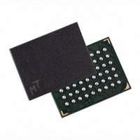
MT45W4MW16BCGB-708 WT Micron Technology Inc, MT45W4MW16BCGB-708 WT Datasheet - Page 18

MT45W4MW16BCGB-708 WT
Manufacturer Part Number
MT45W4MW16BCGB-708 WT
Description
IC PSRAM 64MBIT 70NS 54VFBGA
Manufacturer
Micron Technology Inc
Datasheet
1.MT45W4MW16BCGB-701_IT.pdf
(69 pages)
Specifications of MT45W4MW16BCGB-708 WT
Format - Memory
RAM
Memory Type
PSRAM (Page)
Memory Size
64M (4M x 16)
Speed
70ns
Interface
Parallel
Voltage - Supply
1.7 V ~ 1.95 V
Operating Temperature
-30°C ~ 85°C
Package / Case
54-VFBGA
Operating Temperature (max)
85C
Mounting
Surface Mount
Operating Temperature Classification
Commercial
Lead Free Status / RoHS Status
Lead free / RoHS Compliant
Low-Power Operation
Standby Mode Operation
Temperature-Compensated Refresh
Partial-Array Refresh
Deep Power-Down Operation
Registers
PDF: 09005aef8247bd51/Source: 09005aef8247bd83
64mb_burst_cr1_5_p25z_133mhz__2.fm - Rev. F 9/07 EN
During standby, the device current consumption is reduced to the level necessary to
perform the DRAM refresh operation. Standby operation occurs when CE# is HIGH.
The device will enter a reduced power state upon completion of a READ or WRITE oper-
ation or when the address and control inputs remain static for an extended period of
time. This mode will continue until a change occurs to the address or control inputs.
Temperature-compensated refresh (TCR) allows for adequate refresh at different
temperatures. This CellularRAM device includes an on-chip temperature sensor that
automatically adjusts the refresh rate according to the operating temperature.
Partial-array refresh (PAR) restricts refresh operation to a portion of the total memory
array. This feature enables the device to reduce standby current by refreshing only that
part of the memory array required by the host system. The refresh options are full array,
one-half array, one-quarter array, one-eighth array, or none of the array. The mapping of
these partitions can start either at the beginning or the end of the address map (see
Table 8 on page 32). READ and WRITE operations to address ranges receiving refresh will
not be affected. Data stored in addresses not receiving refresh will become corrupted.
When reenabling additional portions of the array, the new portions are available imme-
diately upon writing to the RCR.
Deep power-down (DPD) operation disables all refresh-related activity. This mode is
used if the system does not require the storage provided by the CellularRAM device. Any
stored data will become corrupted when DPD is enabled. When refresh activity has been
reenabled by rewriting, the CellularRAM device will require 150µs to perform an initial-
ization procedure before normal operations can resume. During this 150µs period, the
current consumption will be higher than the specified standby levels but considerably
lower than the active current specification.
DPD can be enabled by writing to the RCR using CRE or the software access sequence;
DPD starts when CE# goes HIGH. DPD is disabled the next time CE# goes LOW and stays
LOW for at least 10µs.
Two user-accessible configuration registers define the device operation. The bus config-
uration register (BCR) defines how the CellularRAM interacts with the system memory bus
and is nearly identical to its counterpart on burst mode Flash devices. The refresh configu-
ration register (RCR) is used to control how refresh is performed on the DRAM array.
These registers are automatically loaded with default settings during power-up and can
be updated any time the devices are operating in a standby state.
The DIDR provides information on the device manufacturer, the CellularRAM genera-
tion, and the specific device configuration. The DIDR is read-only.
64Mb: 4 Meg x 16 Async/Page/Burst CellularRAM 1.5 Memory
18
Micron Technology, Inc., reserves the right to change products or specifications without notice.
Low-Power Operation
©2005 Micron Technology, Inc. All rights reserved.


