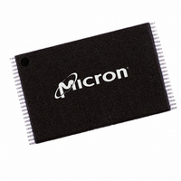
MT28F800B5WG-8 T Micron Technology Inc, MT28F800B5WG-8 T Datasheet - Page 11

MT28F800B5WG-8 T
Manufacturer Part Number
MT28F800B5WG-8 T
Description
IC FLASH 8MBIT 80NS 48TSOP
Manufacturer
Micron Technology Inc
Datasheet
1.MT28F008B5VG-8_B.pdf
(30 pages)
Specifications of MT28F800B5WG-8 T
Format - Memory
FLASH
Memory Type
FLASH - Nor
Memory Size
8M (1M x 8 or 512K x 16)
Speed
80ns
Interface
Parallel
Voltage - Supply
4.5 V ~ 5.5 V
Operating Temperature
0°C ~ 70°C
Package / Case
48-TSOP
Lead Free Status / RoHS Status
Contains lead / RoHS non-compliant
COMMAND SET
MT28F800B5 and MT28F008B5 incorporate an ISM
that controls all internal algorithms for writing and
erasing the floating gate memory cells. An 8-bit com-
mand set is used to control the device. Details on how
to sequence commands are provided in the Command
Execution section. Table 1 lists the valid commands.
ISM STATUS REGISTER
to check for WRITE or ERASE completion or any
related errors. During or following a WRITE, ERASE or
ERASE SUSPEND, a READ operation outputs the status
register contents on DQ0–DQ7 without prior com-
mand. While the status register contents are read, the
outputs are not updated if there is a change in the ISM
status unless OE# or CE# is toggled. If the device is not
Table 2:
09005aef8075d1ec
MT28F800B5_4.fm - Rev. 4, Pub. 2/2004
STATUS
To simplify writing of the memory blocks, the
The 8-bit ISM status register (see Table 2) is polled
BIT #
SR0-2
SR7
SR6
SR5
SR4
SR3
STATUS REGISTER BIT
ISM STATUS
1 = Ready
0 = Busy
ERASE SUSPEND STATUS
1 = ERASE suspended
0 = ERASE in progress/completed
ERASE STATUS
1 = BLOCK ERASE error
0 = Successful BLOCK ERASE
WRITE STATUS
1 = WORD/BYTE WRITE error
0 = Successful WORD/BYTE WRITE
V
1 = No V
0 = V
RESERVED
PP
Status Register
STATUS
PP
present
PP
voltage detected
DESCRIPTION
The ISMS bit displays the active status of the state machine during
WRITE or BLOCK ERASE operations. The controlling logic polls this bit
to determine when the erase and write status bits are valid.
Issuing an ERASE SUSPEND places the ISM in the suspend mode and
sets this and the ISMS bit to “1.” The ESS bit remains “1” until an
ERASE RESUME is issued.
ES is set to “1” after the maximum number of ERASE cycles is executed
by the ISM without a successful verify. ES is only cleared by a CLEAR
STATUS REGISTER command or after a RESET.
WS is set to “1” after the maximum number of WRITE cycles is
executed by the ISM without a successful verify. WS is only cleared by a
CLEAR STATUS REGISTER command or after a RESET.
V
continuously, nor does it indicate a valid V
sampled for 5V after WRITE or ERASE CONFIRM is given. V
cleared by CLEAR STATUS REGISTER or by a RESET.
Reserved for future use.
SMART 5 BOOT BLOCK FLASH MEMORY
PP
S detects the presence of a V
11
in the write, erase, erase suspend or status register read
mode, READ STATUS REGISTER (70h) can be issued to
view the status register contents.
the ISM and erase suspend status bits are reset by the
ISM. The erase, write and V
cleared using CLEAR STATUS REGISTER. If the V
tus bit (SR3) is set, the CEL does not allow further write
or erase operations until the status register is cleared.
This enables the user to choose when to poll and clear
the status register. For example, the host system may
perform multiple BYTE WRITE operations before
checking the status register instead of checking after
each individual WRITE. Asserting the RP# signal or
powering down the device also clears the status regis-
ter.
All of the defined bits are set by the ISM, but only
Micron Technology, Inc., reserves the right to change products or specifications without notice.
PP
voltage. It does not monitor V
PP
voltage. The V
PP
status bits must be
©2002 Micron Technology Inc.
PP
PP
S must be
8Mb
pin is
PP
PP
sta-


