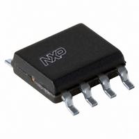
PCF85116-3T/01,118 NXP Semiconductors, PCF85116-3T/01,118 Datasheet - Page 6

PCF85116-3T/01,118
Manufacturer Part Number
PCF85116-3T/01,118
Description
IC EEPROM 16KBIT 400KHZ 8SOIC
Manufacturer
NXP Semiconductors
Datasheet
1.PCF85116-3T01112.pdf
(21 pages)
Specifications of PCF85116-3T/01,118
Format - Memory
EEPROMs - Serial
Memory Type
EEPROM
Memory Size
16K (2K x 8)
Speed
400kHz
Interface
I²C, 2-Wire Serial
Voltage - Supply
2.7 V ~ 5.5 V
Operating Temperature
-40°C ~ 85°C
Package / Case
8-SOIC (3.9mm Width)
For Use With
568-3615 - DEMO BOARD I2C
Lead Free Status / RoHS Status
Lead free / RoHS Compliant
Other names
935233310118
PCF85116-3D-T
PCF85116-3D-T
PCF85116-3D-T
PCF85116-3D-T
Philips Semiconductors
9397 750 14217
Product data
8.1.3 Device addressing
8.1.4 Write operations
The master receiver must generate an acknowledge after the reception of each byte
that has been clocked out of the slave transmitter.
The device that acknowledges has to pull down the SDA line during the acknowledge
clock pulse in such a way that the SDA line is stable LOW during the HIGH period of
the acknowledge related clock pulse.
Set-up and hold times must be taken into account. A master receiver must signal an
end of data to the slave transmitter by not generating an acknowledge on the last byte
that has been clocked out of the slave. In this event, the transmitter must leave the
data line HIGH to enable the master generation of the STOP condition.
Following a START condition, the bus master must output the address of the slave it
is accessing. The four MSBs of the slave address are the device type identifier (see
Figure
The next three significant bits of the slave address field (B3, B2, B1) are the block
selection bits. It is used by the host to select one out of eight blocks
(1 block = 256 bytes of memory). These are, in effect, the three most significant bits
of the word address.
The last bit of the slave address (R/W) defines the operation to be performed. When
R/W is set to logic 1, a read operation is selected.
Byte/word write:
field. This address field is a word address providing access to any one of the eight
blocks of memory. Upon receipt of the word address, the PCF85116-3 responds with
an acknowledge and awaits the next eight bits of data, again responding with an
acknowledge. Word address is automatically incremented. The master can now
terminate the transfer by generating a STOP condition.
After this STOP condition, the E/W cycle starts and the bus is free for another
transmission. Its duration is a maximum of 10 ms.
During the E/W cycle the slave receiver does not send an acknowledge bit if
addressed via the I
Page write:
initiated in the same manner as the byte write operation. The master can transmit up
to 32 data bytes within one transmission. After receipt of each byte, the PCF85116-3
will respond with an acknowledge. The master terminates the transfer by generating a
STOP condition. The maximum total E/W time in this mode is 10 ms.
Fig 3. Slave address.
3). For the PCF85116-3 this is fixed to ‘1010’.
The PCF85116-3 is capable of a 32-byte page write operation. It is
Rev. 04 — 25 October 2004
For a write operation, the PCF85116-3 requires a second address
2
C-bus.
2048
8-bit CMOS EEPROM with I
© Koninklijke Philips Electronics N.V. 2004. All rights reserved.
PCF85116-3
2
C-bus interface
6 of 21


