PSD834F2-90M STMicroelectronics, PSD834F2-90M Datasheet - Page 15
PSD834F2-90M
Manufacturer Part Number
PSD834F2-90M
Description
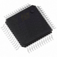
IC FLASH 2MBIT 90NS 52QFP
Manufacturer
STMicroelectronics
Datasheet
1.PSD813F2VA-20JI.pdf
(109 pages)
Specifications of PSD834F2-90M
Format - Memory
FLASH
Memory Type
FLASH
Memory Size
2M (256K x 8)
Speed
90ns
Interface
Parallel
Voltage - Supply
4.5 V ~ 5.5 V
Operating Temperature
0°C ~ 70°C
Package / Case
52-QFP
Lead Free Status / RoHS Status
Lead free / RoHS Compliant
Other names
497-2008
Available stocks
Company
Part Number
Manufacturer
Quantity
Price
Company:

Part Number:
PSD834F2-90M
Manufacturer:
ROCKCHIP
Quantity:
1 302
Company:
Part Number:
PSD834F2-90M
Manufacturer:
ST
Quantity:
490
Company:
Part Number:
PSD834F2-90M
Manufacturer:
STMicroelectronics
Quantity:
10 000
Part Number:
PSD834F2-90M
Manufacturer:
ST
Quantity:
20 000
Company:
Part Number:
PSD834F2-90MI
Manufacturer:
ACTIVE
Quantity:
12 000
Company:
Part Number:
PSD834F2-90MI
Manufacturer:
WSI
Quantity:
10
Company:
Part Number:
PSD834F2-90MI
Manufacturer:
STMicroelectronics
Quantity:
10 000


PSD ARCHITECTURAL OVERVIEW
PSD devices contain several major functional
blocks. Figure
device family. The functions of each block are de-
scribed briefly in the following sections. Many of
the blocks perform multiple functions and are user
configurable.
Memory
Each of the memory blocks is briefly discussed in
the following paragraphs. A more detailed discus-
sion can be found in the section entitled
Blocks, page
The 1 Mbit or 2 Mbit (128K x 8, or 256K x 8) Flash
memory is the primary memory of the PSD. It is di-
vided into 8 equally-sized sectors that are individ-
ually selectable.
The optional 256 Kbit (32K x 8) secondary Flash
memory is divided into 4 equally-sized sectors.
Each sector is individually selectable.
The optional SRAM is intended for use as a
scratch-pad memory or as an extension to the
MCU SRAM.
Each sector of memory can be located in a differ-
ent address space as defined by the user. The ac-
cess times for all memory types includes the
address latching and DPLD decoding time.
Page Register
The 8-bit Page Register expands the address
range of the MCU by up to 256 times. The paged
address can be used as part of the address space
to access external memory and peripherals, or in-
ternal memory and I/O. The Page Register can
also be used to change the address mapping of
sectors of the Flash memories into different mem-
ory spaces for IAP.
PLDs
The device contains two PLDs, the Decode PLD
(DPLD) and the Complex PLD (CPLD), as shown
in Table 3, each optimized for a different function.
The functional partitioning of the PLDs reduces
power consumption, optimizes cost/performance,
and eases design entry.
The DPLD is used to decode addresses and to
generate Sector Select signals for the PSD inter-
19.
5
shows the architecture of the PSD
Doc ID 10552 Rev 3
Memory
nal memory and registers. The DPLD has combi-
natorial outputs. The CPLD has 16 Output
Macrocells (OMC) and 3 combinatorial outputs.
The PSD also has 24 Input Macrocells (IMC) that
can be configured as inputs to the PLDs. The
PLDs receive their inputs from the PLD Input Bus
and are differentiated by their output destinations,
number of product terms, and macrocells.
The PLDs consume minimal power. The speed
and power consumption of the PLD is controlled
by the Turbo Bit in PMMR0 and other bits in the
PMMR2. These registers are set by the MCU at
run-time. There is a slight penalty to PLD propaga-
tion time when invoking the power management
features.
I/O Ports
The PSD has 27 individually configurable I/O pins
distributed over the four ports (Port A, B, C, and
D). Each I/O pin can be individually configured for
different functions. Ports can be configured as
standard MCU I/O ports, PLD I/O, or latched ad-
dress outputs for MCUs using multiplexed ad-
dress/data buses.
The JTAG pins can be enabled on Port C for In-
System Programming (ISP).
Ports A and B can also be configured as a data
port for a non-multiplexed bus.
MCU Bus Interface
PSD interfaces easily with most 8-bit MCUs that
have either multiplexed or non-multiplexed ad-
dress/data buses. The device is configured to re-
spond to the MCU’s control signals, which are also
used as inputs to the PLDs. For examples, please
see the section entitled
Examples, page
Table 3. PLD I/O
Decode PLD (DPLD)
Complex PLD (CPLD)
Name
45.
PSD813F2V, PSD854F2V
73
73
Inputs
MCU Bus Interface
17
19
Outputs
42
140
Product
Terms
15/109
Related parts for PSD834F2-90M
Image
Part Number
Description
Manufacturer
Datasheet
Request
R

Part Number:
Description:
Flash In-System Programmable (ISP) Peripherals for 8-bit MCUs, 5V
Manufacturer:
STMicroelectronics
Datasheet:

Part Number:
Description:
IC FLASH 2MBIT 90NS 52PLCC
Manufacturer:
STMicroelectronics
Datasheet:

Part Number:
Description:
IC FLASH 2MBIT 70NS 52QFP
Manufacturer:
STMicroelectronics
Datasheet:
Part Number:
Description:
IC FLASH 2MBIT 70NS 52PLCC
Manufacturer:
STMicroelectronics
Datasheet:
Part Number:
Description:
IC FLASH 2MBIT 90NS 52PLCC
Manufacturer:
STMicroelectronics
Datasheet:
Part Number:
Description:
IC FLASH 2MBIT 90NS 52QFP
Manufacturer:
STMicroelectronics
Datasheet:
Part Number:
Description:
Manufacturer:
STMicroelectronics
Datasheet:
Part Number:
Description:
Manufacturer:
STMicroelectronics
Datasheet:

Part Number:
Description:
Three Phase Rectifier Bridge
Manufacturer:
POWERSEM [Powersem GmbH]
Datasheet:
Part Number:
Description:
STMicroelectronics [RIPPLE-CARRY BINARY COUNTER/DIVIDERS]
Manufacturer:
STMicroelectronics
Datasheet:
Part Number:
Description:
STMicroelectronics [LIQUID-CRYSTAL DISPLAY DRIVERS]
Manufacturer:
STMicroelectronics
Datasheet:

Part Number:
Description:
BOARD EVAL FOR MEMS SENSORS
Manufacturer:
STMicroelectronics
Datasheet: