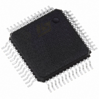
PSD834F2-90M STMicroelectronics, PSD834F2-90M Datasheet - Page 30

PSD834F2-90M
Manufacturer Part Number
PSD834F2-90M
Description
IC FLASH 2MBIT 90NS 52QFP
Manufacturer
STMicroelectronics
Datasheet
1.PSD813F2VA-20JI.pdf
(109 pages)
Specifications of PSD834F2-90M
Format - Memory
FLASH
Memory Type
FLASH
Memory Size
2M (256K x 8)
Speed
90ns
Interface
Parallel
Voltage - Supply
4.5 V ~ 5.5 V
Operating Temperature
0°C ~ 70°C
Package / Case
52-QFP
Lead Free Status / RoHS Status
Lead free / RoHS Compliant
Other names
497-2008
Available stocks
Company
Part Number
Manufacturer
Quantity
Price
Company:
Part Number:
PSD834F2-90M
Manufacturer:
ROCKCHIP
Quantity:
1 302
Company:
Part Number:
PSD834F2-90M
Manufacturer:
ST
Quantity:
490
Company:
Part Number:
PSD834F2-90M
Manufacturer:
STMicroelectronics
Quantity:
10 000
Part Number:
PSD834F2-90M
Manufacturer:
ST
Quantity:
20 000
Company:
Part Number:
PSD834F2-90MI
Manufacturer:
ACTIVE
Quantity:
12 000
Company:
Part Number:
PSD834F2-90MI
Manufacturer:
WSI
Quantity:
10
Company:
Part Number:
PSD834F2-90MI
Manufacturer:
STMicroelectronics
Quantity:
10 000
PSD813F2V, PSD854F2V
SECTOR SELECT AND SRAM SELECT
Sector Select (FS0-FS7, CSBOOT0-CSBOOT3)
and SRAM Select (RS0) are all outputs of the
DPLD. They are setup by writing equations for
them in PSDabel. The following rules apply to the
equations for these signals:
1. Primary Flash memory and secondary Flash
2. Any primary Flash memory sector must not be
3. A secondary Flash memory sector must not be
4. SRAM, I/O, and Peripheral I/O spaces must
5. A secondary Flash memory sector may
6. SRAM, I/O, and Peripheral I/O spaces may
Example
FS0 is valid when the address is in the range of
8000h to BFFFh, CSBOOT0 is valid from 8000h to
9FFFh, and RS0 is valid from 8000h to 87FFh.
Any address in the range of RS0 always accesses
the SRAM. Any address in the range of CSBOOT0
greater than 87FFh (and less than 9FFFh) auto-
matically addresses secondary Flash memory
segment 0. Any address greater than 9FFFh ac-
cesses the primary Flash memory segment 0. You
can see that half of the primary Flash memory seg-
ment 0 and one-fourth of secondary Flash memory
segment 0 cannot be accessed in this example.
Also note that an equation that defined FS1 to any-
where in the range of 8000h to BFFFh would not
be valid.
Figure
components. Any component on a higher level can
overlap and has priority over any component on a
lower level. Components on the same level must
not overlap. Level one has the highest priority and
level 3 has the lowest.
Memory Select Configuration for MCUs with
Separate Program and Data Spaces
The 8031 and compatible family of MCUs, which
includes the 80C51, 80C151, 80C251, and
80C51XA, have separate address spaces for Pro-
gram memory (selected using Program Select En-
able (PSEN, CNTL2)) and Data memory (selected
using Read Strobe (RD, CNTL1)). Any of the
memories within the PSD can reside in either
space or both spaces.
30/109
memory Sector Select signals must not be
larger than the physical sector size.
mapped in the same memory space as
another Flash memory sector.
mapped in the same memory space as
another secondary Flash memory sector.
not overlap.
overlap a primary Flash memory sector. In
case of overlap, priority is given to the
secondary Flash memory sector.
overlap any other memory sector. Priority is
given to the SRAM, I/O, or Peripheral I/O.
9
shows the priority levels for all memory
Doc ID 10552 Rev 3
This is controlled through manipulation of the VM
register that resides in the CSIOP space.
The VM register is set using PSDsoft Express to
have an initial value. It can subsequently be
changed by the MCU so that memory mapping
can be changed on-the-fly.
For example, you may wish to have SRAM and pri-
mary Flash memory in the Data space at Boot-up,
and secondary Flash memory in the Program
space at Boot-up, and later swap the primary and
secondary Flash memories. This is easily done
with the VM register by using PSDsoft Express
Configuration to configure it for Boot-up and hav-
ing the MCU change it when desired.
13., page 31
Figure 9. Priority Level of Memory and I/O
Components
Configuration Modes for MCUs with Separate
Program and Data Spaces
Separate Space Modes. Program space is sep-
arated from Data space. For example, Program
Select Enable (PSEN, CNTL2) is used to access
the program code from the primary Flash memory,
while Read Strobe (RD, CNTL1) is used to access
data from the secondary Flash memory, SRAM
and I/O Port blocks. This configuration requires
the VM register to be set to 0Ch (see
10., page
Combined Space Modes. The
Data spaces are combined into one memory
space that allows the primary Flash memory, sec-
ondary Flash memory, and SRAM to be accessed
by either Program Select Enable (PSEN, CNTL2)
or Read Strobe (RD, CNTL1). For example, to
configure the primary Flash memory in Combined
space, Bits b2 and b4 of the VM register are set to
'1' (see
Highest Priority
Lowest Priority
Figure 11., page
31).
describes the VM Register.
Primary Flash Memory
Non-Volatile Memory
SRAM, I /O, or
Peripheral I /O
Secondary
Level 1
Level 2
Level 3
31).
Program
AI02867D
Figure
Table
and


