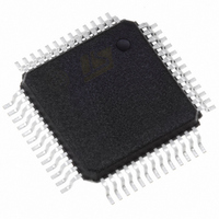
PSD834F2-90M STMicroelectronics, PSD834F2-90M Datasheet - Page 53

PSD834F2-90M
Manufacturer Part Number
PSD834F2-90M
Description
IC FLASH 2MBIT 90NS 52QFP
Manufacturer
STMicroelectronics
Datasheet
1.PSD813F2VA-20JI.pdf
(109 pages)
Specifications of PSD834F2-90M
Format - Memory
FLASH
Memory Type
FLASH
Memory Size
2M (256K x 8)
Speed
90ns
Interface
Parallel
Voltage - Supply
4.5 V ~ 5.5 V
Operating Temperature
0°C ~ 70°C
Package / Case
52-QFP
Lead Free Status / RoHS Status
Lead free / RoHS Compliant
Other names
497-2008
Available stocks
Company
Part Number
Manufacturer
Quantity
Price
Company:
Part Number:
PSD834F2-90M
Manufacturer:
ROCKCHIP
Quantity:
1 302
Company:
Part Number:
PSD834F2-90M
Manufacturer:
ST
Quantity:
490
Company:
Part Number:
PSD834F2-90M
Manufacturer:
STMicroelectronics
Quantity:
10 000
Part Number:
PSD834F2-90M
Manufacturer:
ST
Quantity:
20 000
Company:
Part Number:
PSD834F2-90MI
Manufacturer:
ACTIVE
Quantity:
12 000
Company:
Part Number:
PSD834F2-90MI
Manufacturer:
WSI
Quantity:
10
Company:
Part Number:
PSD834F2-90MI
Manufacturer:
STMicroelectronics
Quantity:
10 000
MCU I/O Mode
In the MCU I/O mode, the MCU uses the I/O Ports
block to expand its own I/O ports. By setting up the
CSIOP space, the ports on the PSD are mapped
into the MCU address space. The addresses of
the ports are listed in
A port pin can be put into MCU I/O mode by writing
a 0 to the corresponding bit in the Control Regis-
ter. The MCU I/O direction may be changed by
writing to the corresponding bit in the Direction
Register, or by the output enable product term.
See
Mode, page
output, the content of the Data Out Register drives
the pin. When configured as an input, the MCU
can read the port input through the Data In buffer.
See
Ports C and D do not have Control Registers, and
are in MCU I/O mode by default. They can be used
for PLD I/O if equations are written for them in PS-
Dabel.
PLD I/O Mode
The PLD I/O Mode uses a port as an input to the
CPLD’s Input Macrocells (IMC), and/or as an out-
put from the CPLD’s Output Macrocells (OMC).
The output can be tri-stated with a control signal.
This output enable control signal can be defined
by a product term from the PLD, or by resetting the
Table 19. Port Operating Modes
Note: 1. Can be multiplexed with other I/O functions.
MCU I/O
PLD I/O
McellAB Outputs
McellBC Outputs
Additional Ext. CS Outputs
PLD Inputs
Address Out
Address In
Data Port
Peripheral I/O
JTAG ISP
Figure 26., page
the
Port Mode
55. When the pin is configured as an
section
Table 7., page
52.
entitled
Yes
Yes
No
No
Yes
Yes (A7 – 0)
Yes
Yes (D7 – 0)
Yes
No
Port A
Peripheral
18.
Doc ID 10552 Rev 3
Yes
Yes
Yes
No
Yes
Yes (A7 – 0)
or (A15 – 8)
Yes
No
No
No
I/O
Port B
corresponding bit in the Direction Register to ’0.’
The corresponding bit in the Direction Register
must not be set to '1' if the pin is defined for a PLD
input signal in PSDabel. The PLD I/O mode is
specified in PSDabel by declaring the port pins,
and then writing an equation assigning the PLD I/
O to a port.
Address Out Mode
For MCUs with a multiplexed address/data bus,
Address Out Mode can be used to drive latched
addresses on to the port pins. These port pins can,
in turn, drive external devices. Either the output
enable or the corresponding bits of both the Direc-
tion Register and Control Register must be set to
a 1 for pins to use Address Out Mode. This must
be done by the MCU at run-time. See Table
the address output pin assignments on Ports A
and B for various MCUs.
For non-multiplexed 8-bit bus mode, address sig-
nals (A7-A0) are available to Port B in Address Out
Mode.
Note: Do not drive address signals with Address
Out Mode to an external memory device if it is in-
tended for the MCU to Boot from the external de-
vice. The MCU must first Boot from PSD memory
so the Direction and Control register bits can be
set.
Yes
No
Yes
No
Yes
No
Yes
No
No
Yes
1
Port C
PSD813F2V, PSD854F2V
Yes
No
No
Yes
Yes
No
Yes
No
No
No
Port D
53/109
21
for


