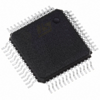
PSD834F2-90M STMicroelectronics, PSD834F2-90M Datasheet - Page 24

PSD834F2-90M
Manufacturer Part Number
PSD834F2-90M
Description
IC FLASH 2MBIT 90NS 52QFP
Manufacturer
STMicroelectronics
Datasheet
1.PSD813F2VA-20JI.pdf
(109 pages)
Specifications of PSD834F2-90M
Format - Memory
FLASH
Memory Type
FLASH
Memory Size
2M (256K x 8)
Speed
90ns
Interface
Parallel
Voltage - Supply
4.5 V ~ 5.5 V
Operating Temperature
0°C ~ 70°C
Package / Case
52-QFP
Lead Free Status / RoHS Status
Lead free / RoHS Compliant
Other names
497-2008
Available stocks
Company
Part Number
Manufacturer
Quantity
Price
Company:
Part Number:
PSD834F2-90M
Manufacturer:
ROCKCHIP
Quantity:
1 302
Company:
Part Number:
PSD834F2-90M
Manufacturer:
ST
Quantity:
490
Company:
Part Number:
PSD834F2-90M
Manufacturer:
STMicroelectronics
Quantity:
10 000
Part Number:
PSD834F2-90M
Manufacturer:
ST
Quantity:
20 000
Company:
Part Number:
PSD834F2-90MI
Manufacturer:
ACTIVE
Quantity:
12 000
Company:
Part Number:
PSD834F2-90MI
Manufacturer:
WSI
Quantity:
10
Company:
Part Number:
PSD834F2-90MI
Manufacturer:
STMicroelectronics
Quantity:
10 000
PSD813F2V, PSD854F2V
Data Polling Flag (DQ7)
When erasing or programming in Flash memory,
the Data Polling Flag Bit (DQ7) outputs the com-
plement of the bit being entered for programming/
writing on the DQ7 Bit. Once the Program instruc-
tion or the WRITE operation is completed, the true
logic value is read on the Data Polling Flag Bit
(DQ7, in a READ operation).
–
–
–
–
Toggle Flag (DQ6)
The PSD offers another way for determining when
the Flash memory Program cycle is completed.
During the internal WRITE operation and when ei-
ther the FS0-FS7 or CSBOOT0-CSBOOT3 is true,
the Toggle Flag Bit (DQ6) toggles from '0' to '1' and
'1' to '0' on subsequent attempts to read any byte
of the memory.
When the internal cycle is complete, the toggling
stops and the data read on the Data Bus D0-D7 is
the addressed memory byte. The device is now
accessible for a new READ or WRITE operation.
The cycle is finished when two successive READs
yield the same output data.
24/109
Data Polling is effective after the fourth WRITE
pulse (for a Program instruction) or after the
sixth WRITE pulse (for an Erase instruction). It
must be performed at the address being
programmed or at an address within the Flash
memory sector being erased.
During an Erase cycle, the Data Polling Flag
Bit (DQ7) outputs a ’0.’ After completion of the
cycle, the Data Polling Flag Bit (DQ7) outputs
the last bit programmed (it is a '1' after
erasing).
If the byte to be programmed is in a protected
Flash memory sector, the instruction is
ignored.
If all the Flash memory sectors to be erased
are protected, the Data Polling Flag Bit (DQ7)
is reset to '0' for about 100µs, and then returns
to the previous addressed byte. No erasure is
performed.
Doc ID 10552 Rev 3
–
–
–
Error Flag (DQ5)
During a normal Program or Erase cycle, the Error
Flag Bit (DQ5) is to ’0.’ This bit is set to '1' when
there is a failure during Flash memory Byte Pro-
gram, Sector Erase, or Bulk Erase cycle.
In the case of Flash memory programming, the Er-
ror Flag Bit (DQ5) indicates the attempt to program
a Flash memory bit from the programmed state,
’0,’ to the erased state, '1,' which is not valid. The
Error Flag Bit (DQ5) may also indicate a Time-out
condition while attempting to program a byte.
In case of an error in a Flash memory Sector Erase
or Byte Program cycle, the Flash memory sector in
which the error occurred or to which the pro-
grammed byte belongs must no longer be used.
Other Flash memory sectors may still be used.
The Error Flag Bit (DQ5) is reset after a Reset
Flash instruction.
Erase Time-out Flag (DQ3)
The Erase Time-out Flag Bit (DQ3) reflects the
time-out period allowed between two consecutive
Sector Erase instructions. The Erase Time-out
Flag Bit (DQ3) is reset to '0' after a Sector Erase
cycle for a time period of 100µs + 20% unless an
additional Sector Erase instruction is decoded. Af-
ter this time period, or when the additional Sector
Erase instruction is decoded, the Erase Time-out
Flag Bit (DQ3) is set to '1.'
The Toggle Flag Bit (DQ6) is effective after the
fourth WRITE pulse (for a Program instruction)
or after the sixth WRITE pulse (for an Erase
instruction).
If the byte to be programmed belongs to a
protected Flash memory sector, the
instruction is ignored.
If all the Flash memory sectors selected for
erasure are protected, the Toggle Flag Bit
(DQ6) toggles to '0' for about 100µs and then
returns to the previous addressed byte.


