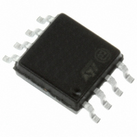
M25P80-VMW6 STMicroelectronics, M25P80-VMW6 Datasheet - Page 18

M25P80-VMW6
Manufacturer Part Number
M25P80-VMW6
Description
IC FLASH 8MBIT 40MHZ 8SOIC
Manufacturer
STMicroelectronics
Datasheet
1.M25P80-VMW6.pdf
(52 pages)
Specifications of M25P80-VMW6
Format - Memory
FLASH
Memory Type
FLASH
Memory Size
8M (1M x 8)
Speed
40MHz
Interface
SPI, 3-Wire Serial
Voltage - Supply
2.7 V ~ 3.6 V
Operating Temperature
-40°C ~ 85°C
Package / Case
8-SOIC (5.3mm Width), 8-SOP, 8-SOEIAJ
Lead Free Status / RoHS Status
Lead free / RoHS Compliant
Other names
497-3601
Available stocks
Company
Part Number
Manufacturer
Quantity
Price
Company:
Part Number:
M25P80-VMW6
Manufacturer:
FREESCALE
Quantity:
13
Part Number:
M25P80-VMW6
Manufacturer:
ST
Quantity:
20 000
Company:
Part Number:
M25P80-VMW6G
Manufacturer:
CET
Quantity:
1 200
Part Number:
M25P80-VMW6G
Manufacturer:
ST
Quantity:
20 000
Part Number:
M25P80-VMW6P
Manufacturer:
AVNET
Quantity:
20 000
Part Number:
M25P80-VMW6T
Manufacturer:
ST
Quantity:
20 000
Company:
Part Number:
M25P80-VMW6TG
Manufacturer:
MICRON
Quantity:
12 500
Company:
Part Number:
M25P80-VMW6TG
Manufacturer:
Numonyx
Quantity:
24 000
Company:
Part Number:
M25P80-VMW6TG
Manufacturer:
MICRON44
Quantity:
7 285
Part Number:
M25P80-VMW6TG
Manufacturer:
MICRON
Quantity:
20 000
Instructions
6
18/52
Instructions
All instructions, addresses and data are shifted in and out of the device, most significant bit
first.
Serial Data Input (D) is sampled on the first rising edge of Serial Clock (C) after Chip Select
(S) is driven Low. Then, the one-byte instruction code must be shifted in to the device, most
significant bit first, on Serial Data input (D), each bit being latched on the rising edges of
Serial Clock (C).
The instruction set is listed in
Every instruction sequence starts with a one-byte instruction code. Depending on the
instruction, this might be followed by address bytes, or by data bytes, or by both or none.
In the case of a Read Data Bytes (READ), Read Data Bytes at Higher Speed (Fast_Read),
Read Status Register (RDSR), Read Identification (RDID) or Release from Deep Power-
down, and Read Electronic Signature (RES) instruction, the shifted-in instruction sequence
is followed by a data-out sequence. Chip Select (S) can be driven High after any bit of the
data-out sequence is being shifted out.
In the case of a Page Program (PP), Sector Erase (SE), Bulk Erase (BE), Write Status
Register (WRSR), Write Enable (WREN), Write Disable (WRDI) or Deep Power-down (DP)
instruction, Chip Select (S) must be driven High exactly at a byte boundary, otherwise the
instruction is rejected, and is not executed. That is, Chip Select (S) must driven High when
the number of clock pulses after Chip Select (S) being driven Low is an exact multiple of
eight.
All attempts to access the memory array during a Write Status Register cycle, Program
cycle or Erase cycle are ignored, and the internal Write Status Register cycle, Program
cycle or Erase cycle continues unaffected.
Table
4.
M25P80


