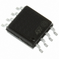
M25P80-VMW6 STMicroelectronics, M25P80-VMW6 Datasheet - Page 35

M25P80-VMW6
Manufacturer Part Number
M25P80-VMW6
Description
IC FLASH 8MBIT 40MHZ 8SOIC
Manufacturer
STMicroelectronics
Datasheet
1.M25P80-VMW6.pdf
(52 pages)
Specifications of M25P80-VMW6
Format - Memory
FLASH
Memory Type
FLASH
Memory Size
8M (1M x 8)
Speed
40MHz
Interface
SPI, 3-Wire Serial
Voltage - Supply
2.7 V ~ 3.6 V
Operating Temperature
-40°C ~ 85°C
Package / Case
8-SOIC (5.3mm Width), 8-SOP, 8-SOEIAJ
Lead Free Status / RoHS Status
Lead free / RoHS Compliant
Other names
497-3601
Available stocks
Company
Part Number
Manufacturer
Quantity
Price
Company:
Part Number:
M25P80-VMW6
Manufacturer:
FREESCALE
Quantity:
13
Part Number:
M25P80-VMW6
Manufacturer:
ST
Quantity:
20 000
Company:
Part Number:
M25P80-VMW6G
Manufacturer:
CET
Quantity:
1 200
Part Number:
M25P80-VMW6G
Manufacturer:
ST
Quantity:
20 000
Part Number:
M25P80-VMW6P
Manufacturer:
AVNET
Quantity:
20 000
Part Number:
M25P80-VMW6T
Manufacturer:
ST
Quantity:
20 000
Company:
Part Number:
M25P80-VMW6TG
Manufacturer:
MICRON
Quantity:
12 500
Company:
Part Number:
M25P80-VMW6TG
Manufacturer:
Numonyx
Quantity:
24 000
Company:
Part Number:
M25P80-VMW6TG
Manufacturer:
MICRON44
Quantity:
7 285
Part Number:
M25P80-VMW6TG
Manufacturer:
MICRON
Quantity:
20 000
M25P80
7
Power-up and Power-down
At Power-up and Power-down, the device must not be selected (that is Chip Select (S) must
follow the voltage applied on V
A safe configuration is provided in
To avoid data corruption and inadvertent write operations during Power-up, a Power On
Reset (POR) circuit is included. The logic inside the device is held reset while V
than the POR threshold value, V
respond to any instruction.
Moreover, the device ignores all Write Enable (WREN), Page Program (PP), Sector Erase
(SE), Bulk Erase (BE) and Write Status Register (WRSR) instructions until a time delay of
t
correct operation of the device is not guaranteed if, by this time, V
No Write Status Register, Program or Erase instructions should be sent until the later of:
These values are specified in
If the delay, t
selected for READ instructions even if the t
At Power-up, the device is in the following state:
Normal precautions must be taken for supply rail decoupling, to stabilize the V
device in a system should have the V
package pins. (Generally, this capacitor is of the order of 100 nF).
At Power-down, when V
(POR) threshold value, V
any instruction. (The designer needs to be aware that if a Power-down occurs while a Write,
Program or Erase cycle is in progress, some data corruption can result.)
PUW
V
V
t
t
The device is in the Standby mode (not the Deep Power-down mode).
The Write Enable Latch (WEL) bit is reset.
The Write In Progress (WIP) bit is reset.
has elapsed after the moment that V
PUW
VSL
CC
SS
(min) at Power-up, and then for a further delay of t
at Power-down
after V
after V
VSL
, has elapsed, after V
CC
CC
passed the V
passed the V
CC
WI
drops from the operating voltage, to below the Power On Reset
, all operations are disabled and the device does not respond to
Table
CC
WI
CC
) until V
WI
Section 3: SPI
– all operations are disabled, and the device does not
(min) level
8.
threshold
CC
CC
rail decoupled by a suitable capacitor close to the
has risen above V
CC
CC
PUW
reaches the correct value:
rises above the V
delay is not yet fully elapsed.
modes.
CC
VSL
(min), the device can be
Power-up and Power-down
WI
CC
threshold. However, the
is still below V
CC
CC
feed. Each
CC
is less
(min).
35/52


