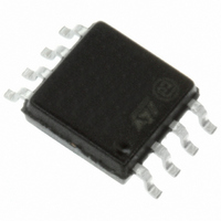
M25P80-VMW6 STMicroelectronics, M25P80-VMW6 Datasheet - Page 28

M25P80-VMW6
Manufacturer Part Number
M25P80-VMW6
Description
IC FLASH 8MBIT 40MHZ 8SOIC
Manufacturer
STMicroelectronics
Datasheet
1.M25P80-VMW6.pdf
(52 pages)
Specifications of M25P80-VMW6
Format - Memory
FLASH
Memory Type
FLASH
Memory Size
8M (1M x 8)
Speed
40MHz
Interface
SPI, 3-Wire Serial
Voltage - Supply
2.7 V ~ 3.6 V
Operating Temperature
-40°C ~ 85°C
Package / Case
8-SOIC (5.3mm Width), 8-SOP, 8-SOEIAJ
Lead Free Status / RoHS Status
Lead free / RoHS Compliant
Other names
497-3601
Available stocks
Company
Part Number
Manufacturer
Quantity
Price
Company:
Part Number:
M25P80-VMW6
Manufacturer:
FREESCALE
Quantity:
13
Part Number:
M25P80-VMW6
Manufacturer:
ST
Quantity:
20 000
Company:
Part Number:
M25P80-VMW6G
Manufacturer:
CET
Quantity:
1 200
Part Number:
M25P80-VMW6G
Manufacturer:
ST
Quantity:
20 000
Part Number:
M25P80-VMW6P
Manufacturer:
AVNET
Quantity:
20 000
Part Number:
M25P80-VMW6T
Manufacturer:
ST
Quantity:
20 000
Company:
Part Number:
M25P80-VMW6TG
Manufacturer:
MICRON
Quantity:
12 500
Company:
Part Number:
M25P80-VMW6TG
Manufacturer:
Numonyx
Quantity:
24 000
Company:
Part Number:
M25P80-VMW6TG
Manufacturer:
MICRON44
Quantity:
7 285
Part Number:
M25P80-VMW6TG
Manufacturer:
MICRON
Quantity:
20 000
Instructions
6.8
28/52
Page Program (PP)
The Page Program (PP) instruction allows bytes to be programmed in the memory
(changing bits from 1 to 0). Before it can be accepted, a Write Enable (WREN) instruction
must previously have been executed. After the Write Enable (WREN) instruction has been
decoded, the device sets the Write Enable Latch (WEL).
The Page Program (PP) instruction is entered by driving Chip Select (S) Low, followed by
the instruction code, three address bytes and at least one data byte on Serial Data input (D).
If the 8 least significant address bits (A7-A0) are not all zero, all transmitted data that goes
beyond the end of the current page are programmed from the start address of the same
page (from the address whose 8 least significant bits (A7-A0) are all zero). Chip Select (S)
must be driven Low for the entire duration of the sequence.
The instruction sequence is shown in
If more than 256 bytes are sent to the device, previously latched data are discarded and the
last 256 data bytes are guaranteed to be programmed correctly within the same page. If less
than 256 Data bytes are sent to device, they are correctly programmed at the requested
addresses without having any effects on the other bytes of the same page.
For optimized timings, it is recommended to use the Page Program (PP) instruction to
program all consecutive targeted bytes in a single sequence versus using several Page
Program (PP) sequences with each containing only a few bytes (see
characteristics (75 MHz operation, Grade
Chip Select (S) must be driven High after the eighth bit of the last data byte has been
latched in, otherwise the Page Program (PP) instruction is not executed.
As soon as Chip Select (S) is driven High, the self-timed Page Program cycle (whose
duration is t
may be read to check the value of the Write In Progress (WIP) bit. The Write In Progress
(WIP) bit is 1 during the self-timed Page Program cycle, and is 0 when it is completed. At
some unspecified time before the cycle is completed, the Write Enable Latch (WEL) bit is
reset.
A Page Program (PP) instruction applied to a page which is protected by the Block Protect
(BP2, BP1, BP0) bits (see
PP
) is initiated. While the Page Program cycle is in progress, the Status Register
Table 3
and
Figure
Table
6)).
14.
2) is not executed.
Table 15: AC
M25P80


