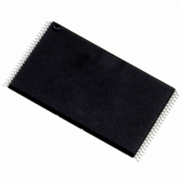
NAND256W3A0AN6E STMicroelectronics, NAND256W3A0AN6E Datasheet - Page 55

NAND256W3A0AN6E
Manufacturer Part Number
NAND256W3A0AN6E
Description
IC FLASH 256MBIT 48TSOP
Manufacturer
STMicroelectronics
Datasheet
1.NAND128W3A2BN6E.pdf
(56 pages)
Specifications of NAND256W3A0AN6E
Format - Memory
FLASH
Memory Type
FLASH - Nand
Memory Size
256M (32M x 8)
Interface
Parallel
Voltage - Supply
2.7 V ~ 3.6 V
Operating Temperature
-40°C ~ 85°C
Package / Case
48-TSOP
Lead Free Status / RoHS Status
Contains lead / RoHS non-compliant
Speed
-
Other names
497-3613
RELATED DOCUMENTATION
STMicroelectronics has published a set of application notes to support the NAND Flash memories. They
are available from the ST Website www.st.com . or from your local ST Distributor.
REVISION HISTORY
Table 29. Document Revision History
06-Jun-2003
07-Aug-2003
27-Oct-2003
03-Dec-2003
13-Apr-2004
28-May-2004
02-Jul-2004
Date
Version
1.0
2.0
3.0
4.0
5.0
6.0
7.0
First Issue
Design Phase
Engineering Phase
Document promoted from Target Specification to Preliminary Data status.
V
Title of
for NANDXXXR3A devices corrected.
WSOP48 and VFBGA55 packages added, VFBGA63 (9 x 11 x 1mm) removed.
Figure 19., Cache Program
for t
Meaning of t
modified in
References removed from
made to ST Website instead.
Figure
paragraph clarified and
modified. Note 2 to
Note 3 to
operations are valid before a Cache Program operation. I
18., DC Characteristics, 1.8V
Waveform. Small text changes.
TFBGA55 package added (mechanical data to be announced). 512Mb Dual Die
devices added.
Package code changed for TFBGA63 8.5 x 15 x 1.2mm, 6x8 ball array, 0.8mm pitch
(1Gbit Dual Die devices) in
Cache Program removed from document. TFBGA55 package specifications added
(Figure 42., TFBGA55 8 x 10mm - 6x8 active ball array - 0.80mm pitch, Package
Outline
Package Mechanical
Test conditions modified for V
Characteristics, 3V
CC
WLWH
changed to V
6.,
Table
and
timing in
Figure
Table 21., AC Characteristics for
Table 7., Address Insertion, x16 Devices
BLBH4
Table 25., TFBGA55 8 x 10mm - 6x8 active ball array - 0.80mm pitch,
2.. changed to
NAND128-A, NAND256-A, NAND512-A, NAND01G-A
Figure 19., Cache Program Operation
7.,
DD
modified, partly replaced by t
Table 20., AC Characteristics for Command, Address, Data
Figure 32., Read C Operation, One Page AC
Devices.
and I
Figure 31.
Data).
CC
Figure 30., Read Electronic Signature AC
Table 28., Ordering Information
Operation, modified and note 2 modified. Note removed
“Product
RELATED DOCUMENTATION
to I
Devices. Note added to
DD
and
Revision Details
.
OL
Figure 34.
Table 1., Product
Description” and Page Program Typical Timing
and V
Operations.
OH
WHBH1
modified.
parameters in
modified.
and t
List, inserted on page 2.
removed. Only 00h Pointer
Figure 34., Block Erase AC
Read Electronic Signature
Scheme.
DD4
WHRL
section and reference
Waveform, removed.
removed from
min for 3V devices
Table 19., DC
Waveform,
Input.
Table
55/56


