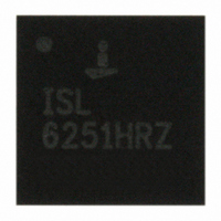
ISL6251HRZ Intersil, ISL6251HRZ Datasheet - Page 17

ISL6251HRZ
Manufacturer Part Number
ISL6251HRZ
Description
IC CTRLR BATT CHRGR LI-ION 28QFN
Manufacturer
Intersil
Datasheet
1.ISL6251HRZ.pdf
(20 pages)
Specifications of ISL6251HRZ
Function
Charge Management
Battery Type
Li-Ion, Li-Pol, NiMH
Voltage - Supply
7 V ~ 25 V
Operating Temperature
-10°C ~ 100°C
Mounting Type
Surface Mount
Package / Case
28-VFQFN Exposed Pad
Lead Free Status / RoHS Status
Lead free / RoHS Compliant
Available stocks
Company
Part Number
Manufacturer
Quantity
Price
Company:
Part Number:
ISL6251HRZ
Manufacturer:
Intersil
Quantity:
135
Company:
Part Number:
ISL6251HRZ
Manufacturer:
Intersil
Quantity:
78
Current loop gain T
equation:
where R
usually equal to the product of the charging current sensing
resistance and the gain of the current sense amplifier, CA2.
For ISL6251, ISL6251A, R
The voltage gain with open current loop is:
T
Where
error amplifier. The Voltage loop gain with current loop
closed is given by:
If T
L
From the above equation, it is shown that the system is a
single order system, which has a single pole located at
before the half switching frequency. Therefore, simple type II
compensator can be easily used to stabilize the system.
Figure 15 shows the voltage loop compensator, and its
transfer function is expressed as follows:
where
T
L
A
V
v
i
v
FIGURE 14. SMALL SIGNAL MODEL OF SYNCHRONOUS
( )
v
+
+
+
+
( )
( )
S
(
S
i
( )
S
S
i ˆ
i ˆ
i ˆ
i ˆ
i ˆ
i ˆ
(S)>>1, then it can be simplified as follows:
v ˆ
v ˆ
v ˆ
v ˆ
v ˆ
v ˆ
S
in
in
in
in
in
in
in
in
in
in
in
in
0.25V
0.25V
)
=
=
=
=
=
ω
K =
1
v ˆ
0.25 R
T
cz
KM F
4 V
-------------- -
v ˆ
T
comp
+
CA2
CA2
V
is the trans-resistance in current loop. R
v
FB
T
=
O
V
F B
( )
11/Vin
11/Vin
I
I
I
I
I
I
V
i
S
L
L
L
L
L
L
FB
( )
d ˆ
d ˆ
d ˆ
d ˆ
d ˆ
d ˆ
R
o
S
BUCK REGULATOR
1
(
----------------------------- -
T
1
+
+
-
-
( )A
R
=
1
C
F
S
, V
1:D
1:D
1:D
1:D
O
d ˆ
d ˆ
d ˆ d ˆ
d ˆ d ˆ
g
1
2
R
m
( )M
+
S
FB
i
V
T
(S) is expressed as the following
1
R
( )
SC
S
+
L
V
V
V
V
V
V
is the feedback voltage of the voltage
)
in
in
in
in
in
in
ω
d ˆ
d ˆ
d ˆ
d ˆ
d ˆ
d ˆ
1
----------------------- - A
S
cz
1
1
T
+
+
= 20R
----------- -
ω
i ˆ
i ˆ
i ˆ
i ˆ
i ˆ
i ˆ
17
L
L
L
L
L
L
T
T
T
T
-------
ω
S
esr
S
i
i
i
i
P
(S)
(S)
(S)
(S)
L
L
L
L
v ˆ
v ˆ
v ˆ
v ˆ
v ˆ
v ˆ
comp
comp
comp
comp
comp
comp
1
V
.
( )
V
V
S
R
R
R
R
CA2
CA2
,
T
T
T
T
-Av(S)
-Av(S)
-Av(S)
-Av(S)
ω
P
≈
---------------- -
R
Rc
Rc
Rc
Rc
Co
Co
O
1
Ro
Ro
Ro
Ro
C
T
T
T
T
v
v
v
v
O
T
(S)
(S)
(S)
(S)
ISL6251, ISL6251A
is
v ˆ
v ˆ
v ˆ
v ˆ
v ˆ
v ˆ
o
o
o
o
o
o
ω
K
K
K
K
p
Compensator design goal:
• High DC gain
• Loop bandwidth f
• Gain margin: >10dB
• Phase margin: 40°
The compensator design procedure is as follows:
The loop gain T
gain. Therefore, the compensator resistance R
determined by:
where g
amplifier. Compensator capacitor C1 is then given by:
Example: V
C
V
R
1.5kHz. The compensator capacitor is C
Therefore, choose voltage loop compensator: R
C
R
C
1. Put compensator zero at:
2. Put one compensator pole at zero frequency to achieve
FB
1
1
o
1
1
=
= 10 μ F/10m Ω , L = 10 μ H, g
= 10k Ω . Choose R
= 6.5nF.
=
high DC gain, and put another compensator pole at either
ESR zero frequency or half switching frequency,
whichever is lower.
ω
= 2.1V, f
R
cz
8 π f
-------------------------------------- -
1
1
m
FIGURE 15. VOLTAGE LOOP COMPENSATOR
ω
=
C
g
cz
m
V
is the trans-conductance of the voltage loop error
(
1 −
in
O
V
c
FB
C
= 19V, V
3
= 20kHz, then compensator resistance
O
)
v
R
(S) at cross over frequency of f
R
T
o
1
c
C
Vo
Vo
Vo
Vo
:
o
V
V
1
V
V
⎛
⎜
⎝
o
REF
REF
FB
FB
1
5
= 10k Ω . Put the compensator zero at
= 16.8V, I
−
20
-
-
-
-
+
+
+
+
1
g
g
⎞
⎟
⎠
m
m
m
f
s
= 250 μ s, R
o
= 2.6A, f
C1
C1
R1
R1
V
V
COMP
COMP
1
= 6.5nF.
T
s
= 300kHz,
= 0.8 Ω ,
1
c
1
is
has unity
= 10k,
May 10, 2006
FN9202.2


