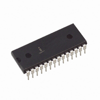
ICL7135CPIZ Intersil, ICL7135CPIZ Datasheet - Page 8

ICL7135CPIZ
Manufacturer Part Number
ICL7135CPIZ
Description
IC ADC 4.5DIGIT MUXED BCD 28DIP
Manufacturer
Intersil
Datasheet
1.ICL7135CPIZ.pdf
(15 pages)
Specifications of ICL7135CPIZ
Display Type
LED, LCD
Configuration
7 Segment
Interface
BCD
Digits Or Characters
A/D 4.5 Digits
Current - Supply
1.1mA
Voltage - Supply
4 V ~ 6 V
Operating Temperature
0°C ~ 70°C
Mounting Type
Through Hole
Package / Case
28-DIP (0.600", 15.24mm)
Lead Free Status / RoHS Status
Lead free / RoHS Compliant
Available stocks
Company
Part Number
Manufacturer
Quantity
Price
Company:
Part Number:
ICL7135CPIZ
Manufacturer:
TI
Quantity:
12 400
Company:
Part Number:
ICL7135CPIZ
Manufacturer:
INTERSIL
Quantity:
28 314
Part Number:
ICL7135CPIZ
Manufacturer:
INTERSIL
Quantity:
20 000
series with the integrating capacitor. The effect of the
resistor is to introduce a small pedestal voltage on to the
integrator output at the beginning of the reference integrate
phase. By careful selection of the ratio between this resistor
and the integrating resistor (a few tens of ohms in the
recommended circuit), the comparator delay can be
compensated and the maximum clock frequency extended
by approximately a factor of 3. At higher frequencies, ringing
and second order breaks will cause significant non-
linearities in the first few counts of the instrument. See
Application Note AN017.
The minimum clock frequency is established by leakage on
the auto-zero and reference caps. With most devices,
measurement cycles as long as 10s give no measurable
leakage error.
To achieve maximum rejection of 60Hz pickup, the signal
integrate cycle should be a multiple of 60Hz. Oscillator
frequencies of 300kHz, 200kHz, 150kHz, 120kHz, 100kHz,
40kHz, 33
rejection, oscillator frequencies of 250kHz, 166
125kHz, 100kHz, etc. would be suitable. Note that 100kHz
(2.5 readings/sec) will reject both 50Hz and 60Hz.
WHEN APPLICABLE
WHEN APPLICABLE
FOR OVER-RANGE
FOR OVER-RANGE
UNDER-RANGE
OVER-RANGE
INTEGRATOR
DIGIT SCAN
DIGIT SCAN
FIGURE 6. TIMING DIAGRAM FOR OUTPUTS
1
STROBE
OUTPUT
/
3
BUSY
kHz, etc. should be selected. For 50Hz
COUNTS
COUNTS
10,001/
EXPANDED SCALE
1000
AUTO
ZERO
D5
D4
AUTO ZERO
CYCLE 40,002 COUNTS
D3
FULL MEASUREMENT
SIGNAL INTEGRATE
†
D2
BELOW
/
D1
COUNTS
SIGNAL
10,000/
INT.
8
REF INT ONE COUNT LONGER
COUNTS MAX.
REFERENCE
INTEGRATE
20,001/
D5
D4
D3
D2
D1
†
FIRST D5 OF AZ AND
2
/
3
REFERENCE
INTEGRATE
kHz,
ICL7135
The clock used should be free from significant phase or
frequency jitter. Several suitable low-cost oscillators are
shown in the Typical Applications section. The multiplexed
output means that if the display takes significant current from
the logic supply, the clock should have good PSRR.
Zero-Crossing Flip-Flop
The flip-flop interrogates the data once every clock pulse
after the transients of the previous clock pulse and half-clock
pulse have died down. False zero-crossings caused by clock
pulses are not recognized. Of course, the flip-flop delays the
true zero-crossing by up to one count in every instance, and
if a correction were not made, the display would always be
one count too high. Therefore, the counter is disabled for
one clock pulse at the beginning of phase 3. This one-count
delay compensates for the delay of the zero-crossing
flip-flop, and allows the correct number to be latched into the
display. Similarly, a one-count delay at the beginning of
phase 1 gives an overload display of 0000 instead of 0001.
No delay occurs during phase 2, so that true ratiometric
readings result.
Evaluating The Error Sources
Errors from the “ideal” cycle are caused by:
Each error is analyzed for its error contribution to the
converter in application notes listed on the back page,
specifically Application Note AN017 and Application Note
AN032.
Noise
The peak-to-peak noise around zero is approximately 15μV
(peak-to-peak value not exceeded 95% of the time). Near
full scale, this value increases to approximately 30μV. Much
of the noise originates in the auto-zero loop, and is
proportional to the ratio of the input signal to the reference.
Analog And Digital Grounds
Extreme care must be taken to avoid ground loops in the
layout of ICL7135 circuits, especially in high-sensitivity
circuits. It is most important that return currents from digital
loads are not fed into the analog ground line.
1. Capacitor droop due to leakage.
2. Capacitor voltage change due to charge “suck-out” (the
3. Non-linearity of buffer and integrator.
4. High-frequency limitations of buffer, integrator, and
5. Integrating capacitor non-linearity (dielectric absorption).
6. Charge lost by C
7. Charge lost by C
reverse of charge injection) when the switches turn off.
comparator.
REF
AZ
and C
in charging C
lNT
to charge C
STRAY
STRAY
.
.
FN3093.4


