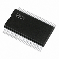
PCF8576T,118 NXP Semiconductors, PCF8576T,118 Datasheet - Page 20

PCF8576T,118
Manufacturer Part Number
PCF8576T,118
Description
IC LCD DVR UNVRSL LOW-MUX 56VSO
Manufacturer
NXP Semiconductors
Datasheet
1.PCF8576DT2118.pdf
(50 pages)
Specifications of PCF8576T,118
Display Type
LCD
Configuration
40 Segment
Interface
I²C
Current - Supply
180µA
Voltage - Supply
2 V ~ 9 V
Operating Temperature
-40°C ~ 85°C
Mounting Type
Surface Mount
Package / Case
56-VSOP
Lead Free Status / RoHS Status
Lead free / RoHS Compliant
Digits Or Characters
-
Other names
933740730118
PCF8576TD-T
PCF8576TD-T
PCF8576TD-T
PCF8576TD-T
NXP Semiconductors
PCF8576D
Product data sheet
7.13 Output bank selector
7.14 Input bank selector
7.15 Blinker
The storage arrangements described lead to extremely efficient data loading in cascaded
applications. When a series of display bytes are sent to the display RAM, automatic
wrap-over to the next PCF8576D occurs when the last RAM address is exceeded.
Subaddressing across device boundaries is successful even if the change to the next
device in the cascade occurs within a transmitted character (such as during the 14
display data byte transmitted in 1:3 multiplex mode).
The hardware subaddress must not be changed while the device is being accessed on the
I
The output bank selector selects one of the four bits per display RAM address for transfer
to the display latch. The actual bit chosen depends on the selected LCD drive mode in
operation and on the instant in the multiplex sequence.
The PCF8576D includes a RAM bank switching feature in the static and 1:2 drive modes.
In the static drive mode, the bank-select command (see
contents of bit 2 to be selected for display instead of the contents of bit 0. In 1:2 mode, the
contents of bits 2 and 3 may be selected instead of bits 0 and 1. This gives the provision
for preparing display information in an alternative bank and to be able to switch to it once
it is assembled.
The input bank selector loads display data into the display RAM in accordance with the
selected LCD drive configuration.
The bank-select command (see
static drive mode or in bits 2 and 3 in 1:2 mode. The input bank selector functions are
independent of the output bank selector.
The PCF8576D has a very versatile display blinking capability. The whole display can
blink at a frequency selected by the blink-select command (see
frequency is a fraction of the clock frequency; the ratio between the clock frequency and
blink frequency depends on the blink mode selected (see
An additional feature allows an arbitrary selection of LCD segments to blink in the static
and 1:2 drive modes. This is implemented without any communication overheads by the
output bank selector which alternates the displayed data between the data in the display
RAM bank and the data in an alternative RAM bank at the blink frequency. This mode can
also be implemented by the blink-select command (see
2
C-bus interface.
•
•
•
•
In 1:4 mode, all RAM addresses of bit 0 are selected, these are followed by the
contents of bit 1, bit 2 and then bit 3.
In 1:3 mode, bits 0, 1 and 2 are selected sequentially
In 1:2 mode, bits 0 and 1 are selected
In static mode, bit 0 is selected
All information provided in this document is subject to legal disclaimers.
Rev. 10 — 14 February 2011
Section
7.17) can be used to load display data in bit 2 in
Universal LCD driver for low multiplex rates
Section
Section
Table
Section
6).
7.17).
7.17) may request the
PCF8576D
© NXP B.V. 2011. All rights reserved.
7.17). Each blink
th
20 of 50


