LP5521TM/NOPB National Semiconductor, LP5521TM/NOPB Datasheet - Page 14
LP5521TM/NOPB
Manufacturer Part Number
LP5521TM/NOPB
Description
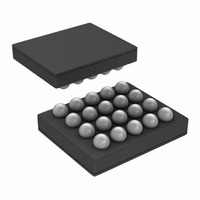
IC LED DRIVER RGB 25-USMD
Manufacturer
National Semiconductor
Series
PowerWise®r
Type
RGB LED Driverr
Datasheet
1.LP5521TMNOPB.pdf
(40 pages)
Specifications of LP5521TM/NOPB
Constant Current
Yes
Topology
PWM, Switched Capacitor (Charge Pump)
Number Of Outputs
3
Internal Driver
Yes
Type - Primary
Backlight, Light Management Unit (LMU)
Type - Secondary
RGB
Frequency
1.25MHz
Voltage - Supply
2.7 V ~ 5.5 V
Voltage - Output
4.55V
Mounting Type
Surface Mount
Package / Case
20-MicroSMD
Operating Temperature
-30°C ~ 85°C
Current - Output / Channel
25.5mA
Internal Switch(s)
Yes
Efficiency
95%
Lead Free Status / RoHS Status
Lead free / RoHS Compliant
Other names
LP5521TMTR
Available stocks
Company
Part Number
Manufacturer
Quantity
Price

Part Number:
LP5521TM/NOPB
Manufacturer:
NS/国半
Quantity:
20 000


www.national.com
Charge Pump Operational Description
OVERVIEW
The LP5521 includes a pre-regulated switched-capacitor
charge pump with a programmable voltage multiplication of 1
and 1.5x.
On 1.5x mode by combining the principles of a switched-ca-
pacitor charge pump and a linear regulator, it generates a
regulated 4.5V output from Li-Ion input voltage range. A two-
phase non-overlapping clock generated internally controls the
operation of the charge pump. During the charge phase, both
flying capacitors (C
voltage. In the pump phase that follows, the flying capacitors
are discharged to output. A traditional switched capacitor
charge pump operating in this manner will use switches with
very low on-resistance, ideally 0Ω, to generate an output volt-
age that is 1.5x the input voltage. The LP5521 regulates the
output voltage by controlling the resistance of the input-con-
nected pass-transistor switches in the charge pump.
OUTPUT RESISTANCE
At lower input voltages, the charge pump output voltage may
degrade due to effective output resistance (R
charge pump. The expected voltage drop can be calculated
by using a simple model for the charge pump illustrated in
following figure.
The model shows a linear pre-regulation block (REG), a volt-
age multiplier (1.5x), and an output resistance (R
resistance models the output voltage drop that is inherent to
switched capacitor converters. The output resistance is 3.5Ω
(typ), and is function of switching frequency, input voltage,
flying capacitors’ capacitance value, internal resistances of
switches and ESR of flying capacitors. When the output volt-
age is in regulation, the regulator in the model controls the
voltage V’ to keep the output voltage equal to 4.5V (typ). With
increased output current, the voltage drop across R
creases. To prevent drop in output voltage, the voltage drop
across the regulator is reduced, V’ increases, and V
mains at 4.5V. When the output current increases to the point
that there is zero voltage drop across the regulator, V’ equals
the input voltage, and the output voltage is “on the edge” of
regulation. Additional output current causes the output volt-
age to fall out of regulation, so that the operation is similar to
a basic open-loop 1.5x charge pump. In this mode, output
current results in output voltage drop proportional to the out-
put resistance of the charge pump. The out-of-regulation
output voltage can be approximated by: V
I
OUT
x R
OUT
.
FLY1
and C
FLY2
) are charged from input
OUT
= 1.5 x V
OUT
OUT
20186297
). Output
) of the
OUT
OUT
IN
re-
in-
–
14
CONTROLLING CHARGE PUMP
Charge pump is controlled with two CP_MODE bits in register
08H. When both bits are low, charge pump is disabled and
output voltage is pulled down with 300 kΩ. Charge pump can
be forced to bypass mode, so battery voltage is going directly
to RGB outputs. In 1.5x mode output voltage is boosted to
4.5V. In automatic mode, charge pump operation mode is
defined by LED outputs saturation like described in LED For-
ward Voltage Monitoring. In following table are listed opera-
tion modes and selection bits.
LED FORWARD VOLTAGE MONITORING
When charge pump automatic mode selection is enabled,
voltages over LED drivers are monitored. If drivers do not
have enough headroom, charge pump gain is set to 1.5x.
Driver saturation monitor does not have a fixed voltage limit,
since saturation voltage is a function of temperature and cur-
rent. Charge pump gain is set to 1x, when battery voltage is
high enough to supply all LEDs.
In automatic gain change mode, charge pump is switched to
bypass mode (1x), when LEDs are inactive for over 50 ms.
Charge pump gain control utilizes digital filtering to prevent
supply voltage disturbances from triggering gain changes. If
R driver current source is connected to battery (address 08H,
bit R_TO_BATT = 1) voltage monitoring is disabled in R out-
put, but still functional in B and G output.
LED forward voltage monitoring and gain control block dia-
gram is shown below.
CP_MODE
Name
Voltage monitoring block diagram for one output
Bit
4:3
CONFIG register (08H):
Description
Charge Pump Operation Mode
00b = OFF
01b = Forced to bypass mode (1x)
10b = Forced to 1.5x mode
11b = Automatic mode selection
20186255
Related parts for LP5521TM/NOPB
Image
Part Number
Description
Manufacturer
Datasheet
Request
R

Part Number:
Description:
Programmable Three Channel LED Driver
Manufacturer:
NSC [National Semiconductor]
Datasheet:

Part Number:
Description:
National Semiconductor [8-Bit D/A Converter]
Manufacturer:
National Semiconductor
Datasheet:
Part Number:
Description:
National Semiconductor [Media Coprocessor]
Manufacturer:
National Semiconductor
Datasheet:
Part Number:
Description:
Digitally Controlled Tone and Volume Circuit with Stereo Audio Power Amplifier, Microphone Preamp Stage and National 3D Sound
Manufacturer:
National Semiconductor
Datasheet:
Part Number:
Description:
Digitally Controlled Tone and Volume Circuit with Stereo Audio Power Amplifier, Microphone Preamp Stage and National 3D Sound
Manufacturer:
National Semiconductor
Datasheet:
Part Number:
Description:
AC97 Rev 2 Codec with Sample Rate Conversion and National 3D Sound
Manufacturer:
National Semiconductor
Part Number:
Description:
Manufacturer:
National Semiconductor
Datasheet:
Part Number:
Description:
Manufacturer:
National Semiconductor
Datasheet:
Part Number:
Description:
General Purpose, Low Voltage, Low Power, Rail-to-Rail Output Operational Amplifiers
Manufacturer:
National Semiconductor
Datasheet:
Part Number:
Description:
8-bit 20 MSPS flash A/D converter.
Manufacturer:
National Semiconductor
Datasheet:
Part Number:
Description:
Low Noise Quad Operational Amplifier
Manufacturer:
National Semiconductor
Datasheet:
Part Number:
Description:
Quad Differential Line Receivers
Manufacturer:
National Semiconductor
Datasheet:
Part Number:
Description:
Quad High Speed Trapezoidal? Bus Transceiver
Manufacturer:
National Semiconductor
Datasheet:
Part Number:
Description:
Dual Line Receiver
Manufacturer:
National Semiconductor
Datasheet: