LP5521TM/NOPB National Semiconductor, LP5521TM/NOPB Datasheet - Page 8
LP5521TM/NOPB
Manufacturer Part Number
LP5521TM/NOPB
Description
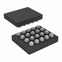
IC LED DRIVER RGB 25-USMD
Manufacturer
National Semiconductor
Series
PowerWise®r
Type
RGB LED Driverr
Datasheet
1.LP5521TMNOPB.pdf
(40 pages)
Specifications of LP5521TM/NOPB
Constant Current
Yes
Topology
PWM, Switched Capacitor (Charge Pump)
Number Of Outputs
3
Internal Driver
Yes
Type - Primary
Backlight, Light Management Unit (LMU)
Type - Secondary
RGB
Frequency
1.25MHz
Voltage - Supply
2.7 V ~ 5.5 V
Voltage - Output
4.55V
Mounting Type
Surface Mount
Package / Case
20-MicroSMD
Operating Temperature
-30°C ~ 85°C
Current - Output / Channel
25.5mA
Internal Switch(s)
Yes
Efficiency
95%
Lead Free Status / RoHS Status
Lead free / RoHS Compliant
Other names
LP5521TMTR
Available stocks
Company
Part Number
Manufacturer
Quantity
Price

Part Number:
LP5521TM/NOPB
Manufacturer:
NS/国半
Quantity:
20 000


www.national.com
I
Note 1: Absolute Maximum Ratings indicate limits beyond which damage to the component may occur. Operating Ratings are conditions under which operation
of the device is guaranteed. Operating Ratings do not imply guaranteed performance limits. For guaranteed performance limits and associated test conditions,
see the Electrical Characteristics tables.
Note 2: All voltages are with respect to the potential at the GND pins.
Note 3: Internal thermal shutdown circuitry protects the device from permanent damage. Thermal shutdown engages at T
= 130°C (typ.).
Note 4: For detailed soldering specifications and information, please refer to National Semiconductor Application Note AN1112 : Micro SMD Wafer Level Chip
Scale Package or AN1187 : Leadless Leadframe Package (LLP).
Note 5: The Human body model is a 100 pF capacitor discharged through a 1.5 kΩ resistor into each pin. The machine model is a 200 pF capacitor discharged
directly into each pin. MIL-STD-883 3015.7
Note 6: In applications where high power dissipation and/or poor package thermal resistance is present, the maximum ambient temperature may have to be
derated. Maximum ambient temperature (T
dissipation of the device in the application (P
following equation: T
Note 7: Junction-to-ambient thermal resistance is highly application and board-layout dependent. In applications where high maximum power dissipation exists,
special care must be paid to thermal dissipation issues in board design.
Note 8: Min and Max limits are guaranteed by design, test, or statistical analysis. Typical numbers are not guaranteed, but do represent the most likely norm.
Note 9: Low-ESR Surface-Mount Ceramic Capacitors (MLCCs) used in setting electrical characteristics.
Note 10: Input, output, and fly capacitors should be of the type X5R or X7R low ESR ceramic capacitor.
Note 11: Matching is the maximum difference from the average of the three output's currents.
Note 12: Saturation voltage is defined as the voltage when the LED current has dropped 10% from the value measured at V
Note 13: Guaranteed by design.
2
Symbol
C Timing Parameters (SDA, SCL)
f
SCL
10
C
1
2
3
4
5
6
7
8
9
b
Clock Frequency
Hold Time (repeated) START Condition
Clock Low Time
Clock High Time
Setup Time for a Repeated START Condition
Data Hold Time
Data Setup Time
Rise Time of SDA and SCL
Fall Time of SDA and SCL
Set-up Time for STOP condition
Bus Free Time between a STOP and a START Condition
Capacitive Load for Each Bus Line
A-MAX
= T
J-MAX-OP
– (θ
JA
A-MAX
× P
D-MAX
D-MAX
) is dependent on the maximum operating junction temperature (T
), and the junction-to ambient thermal resistance of the part/package in the application (θ
Parameter
).
(Note 13)
8
20+0.1C
15+0.1C
Min
600
600
100
600
0.6
1.3
1.3
50
10
J-MAX-OP
b
b
Limit
J
= 125°C), the maximum power
= 150°C (typ.) and disengages at T
OUT
- 1V.
Max
400
300
300
200
20186298
JA
), as given by the
Units
kHz
µs
µs
ns
ns
ns
ns
ns
ns
ns
µs
pF
J
Related parts for LP5521TM/NOPB
Image
Part Number
Description
Manufacturer
Datasheet
Request
R

Part Number:
Description:
Programmable Three Channel LED Driver
Manufacturer:
NSC [National Semiconductor]
Datasheet:

Part Number:
Description:
National Semiconductor [8-Bit D/A Converter]
Manufacturer:
National Semiconductor
Datasheet:
Part Number:
Description:
National Semiconductor [Media Coprocessor]
Manufacturer:
National Semiconductor
Datasheet:
Part Number:
Description:
Digitally Controlled Tone and Volume Circuit with Stereo Audio Power Amplifier, Microphone Preamp Stage and National 3D Sound
Manufacturer:
National Semiconductor
Datasheet:
Part Number:
Description:
Digitally Controlled Tone and Volume Circuit with Stereo Audio Power Amplifier, Microphone Preamp Stage and National 3D Sound
Manufacturer:
National Semiconductor
Datasheet:
Part Number:
Description:
AC97 Rev 2 Codec with Sample Rate Conversion and National 3D Sound
Manufacturer:
National Semiconductor
Part Number:
Description:
Manufacturer:
National Semiconductor
Datasheet:
Part Number:
Description:
Manufacturer:
National Semiconductor
Datasheet:
Part Number:
Description:
General Purpose, Low Voltage, Low Power, Rail-to-Rail Output Operational Amplifiers
Manufacturer:
National Semiconductor
Datasheet:
Part Number:
Description:
8-bit 20 MSPS flash A/D converter.
Manufacturer:
National Semiconductor
Datasheet:
Part Number:
Description:
Low Noise Quad Operational Amplifier
Manufacturer:
National Semiconductor
Datasheet:
Part Number:
Description:
Quad Differential Line Receivers
Manufacturer:
National Semiconductor
Datasheet:
Part Number:
Description:
Quad High Speed Trapezoidal? Bus Transceiver
Manufacturer:
National Semiconductor
Datasheet:
Part Number:
Description:
Dual Line Receiver
Manufacturer:
National Semiconductor
Datasheet: