LP5521TM/NOPB National Semiconductor, LP5521TM/NOPB Datasheet - Page 6
LP5521TM/NOPB
Manufacturer Part Number
LP5521TM/NOPB
Description
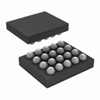
IC LED DRIVER RGB 25-USMD
Manufacturer
National Semiconductor
Series
PowerWise®r
Type
RGB LED Driverr
Datasheet
1.LP5521TMNOPB.pdf
(40 pages)
Specifications of LP5521TM/NOPB
Constant Current
Yes
Topology
PWM, Switched Capacitor (Charge Pump)
Number Of Outputs
3
Internal Driver
Yes
Type - Primary
Backlight, Light Management Unit (LMU)
Type - Secondary
RGB
Frequency
1.25MHz
Voltage - Supply
2.7 V ~ 5.5 V
Voltage - Output
4.55V
Mounting Type
Surface Mount
Package / Case
20-MicroSMD
Operating Temperature
-30°C ~ 85°C
Current - Output / Channel
25.5mA
Internal Switch(s)
Yes
Efficiency
95%
Lead Free Status / RoHS Status
Lead free / RoHS Compliant
Other names
LP5521TMTR
Available stocks
Company
Part Number
Manufacturer
Quantity
Price

Part Number:
LP5521TM/NOPB
Manufacturer:
NS/国半
Quantity:
20 000


www.national.com
R
f
I
t
V
Symbol
SW
GND
ON
OUT
OUT
Absolute Maximum Ratings
If Military/Aerospace specified devices are required,
please contact the National Semiconductor Sales Office/
Distributors for availability and specifications.
Electrical Characteristics
Limits in standard typeface are for T
< T
1 μF, C
Charge Pump Electrical Characteristics
I
f
VDD
OSC
V(V
Voltage on Logic Pins
Continuous Power Dissipation
(Note 3)
Junction Temperature (T
Storage Temperature Range
Maximum Lead Temperature
(Soldering)
ESD Rating (Note 5)
Human Body Model:
Machine Model:
Symbol
A
< +85°C). Unless otherwise noted, specifications apply to the LP5521 Block Diagram with: 2.7V
DD
FLY1
, V
Standby supply
current
Normal mode
supply current
Powersave mode
supply current
Internal oscillator
frequency accuracy
OUT
= C
Parameter
, R, G, B)
FLY2
Charge pump output resistance
Switching frequency
Ground current
V
off to 1.5x mode
Charge pump output voltage
OUT
= 0.47 μF. (Note 9).
turn-on time from charge pump
J-MAX
EN = 0 (pin), CHIP_EN = 0 (bit), external 32 kHz clock running or not
running
EN = 1 (pin), CHIP_EN = 0 (bit), external 32 kHz clock not running
EN = 1 (pin), CHIP_EN = 0 (bit), external 32 kHz clock running
Charge pump and LED drivers disabled
Charge pump in 1x mode, no load, LED drivers disabled
Charge pump in 1.5x mode, no load, LED drivers disabled
Charge pump in 1x mode, no load, LED drivers enabled
External 32 kHz clock running
Internal oscillator running
Parameter
)
J
= 25°C. Limits in boldface type apply over the operating ambient temperature range (-30°C
-0.3V to V
Internally Limited
-65°C to +150°C
-0.3V to +6.0V
(Notes 2, 8)
with 6.0V max
(Notes 1, 2)
DD
(Note 4)
125°C
+0.3V
200V
2 kV
Gain = 1.5x
Gain = 1x
Gain = 1.5x
Gain = 1x
V
I
V
OUT
DD
DD
= 3.6V, CHIP_EN = H
= 3.6V, no load, Gain = 1.5x
Condition
= 60 mA
6
(Note 10)
Operating Ratings
Thermal Properties
Condition
V
Recommended Charge Pump
Load Current I
Junction Temperature (T
Ambient Temperature (T
(Note 6)
Junction-to-Ambient Thermal
Resistance (θ
(Note 7)
Junction-to-Ambient Thermal
Resistance (θ
(Note 7)
DD
JA
JA
OUT
), TMD20 Package
), YQA24A Package
A
J
) Range
) Range
Min
-7
(Notes 1, 2)
≤
V
Min
-4
-7
DD
1.25
4.55
Typ
100
3.5
1.2
0.5
1
≤
5.5V, C
-30°C to +125°C
0.25
0.70
0.25
Typ
0.2
1.0
1.4
1.5
1.2
10
-30°C to +85°C
50 - 90°C/W
37 - 90°C/W
Max
0 to 100 mA
2.7 to 5.5V
7
OUT
Max Units
2
4
7
= C
Units
MHz
IN
mA
mA
μs
%
Ω
Ω
V
mA
mA
mA
mA
mA
μA
μA
μA
μA
%
=
Related parts for LP5521TM/NOPB
Image
Part Number
Description
Manufacturer
Datasheet
Request
R

Part Number:
Description:
Programmable Three Channel LED Driver
Manufacturer:
NSC [National Semiconductor]
Datasheet:

Part Number:
Description:
National Semiconductor [8-Bit D/A Converter]
Manufacturer:
National Semiconductor
Datasheet:
Part Number:
Description:
National Semiconductor [Media Coprocessor]
Manufacturer:
National Semiconductor
Datasheet:
Part Number:
Description:
Digitally Controlled Tone and Volume Circuit with Stereo Audio Power Amplifier, Microphone Preamp Stage and National 3D Sound
Manufacturer:
National Semiconductor
Datasheet:
Part Number:
Description:
Digitally Controlled Tone and Volume Circuit with Stereo Audio Power Amplifier, Microphone Preamp Stage and National 3D Sound
Manufacturer:
National Semiconductor
Datasheet:
Part Number:
Description:
AC97 Rev 2 Codec with Sample Rate Conversion and National 3D Sound
Manufacturer:
National Semiconductor
Part Number:
Description:
Manufacturer:
National Semiconductor
Datasheet:
Part Number:
Description:
Manufacturer:
National Semiconductor
Datasheet:
Part Number:
Description:
General Purpose, Low Voltage, Low Power, Rail-to-Rail Output Operational Amplifiers
Manufacturer:
National Semiconductor
Datasheet:
Part Number:
Description:
8-bit 20 MSPS flash A/D converter.
Manufacturer:
National Semiconductor
Datasheet:
Part Number:
Description:
Low Noise Quad Operational Amplifier
Manufacturer:
National Semiconductor
Datasheet:
Part Number:
Description:
Quad Differential Line Receivers
Manufacturer:
National Semiconductor
Datasheet:
Part Number:
Description:
Quad High Speed Trapezoidal? Bus Transceiver
Manufacturer:
National Semiconductor
Datasheet:
Part Number:
Description:
Dual Line Receiver
Manufacturer:
National Semiconductor
Datasheet: