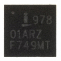
ISL97801ARZ-TK Intersil, ISL97801ARZ-TK Datasheet - Page 12

ISL97801ARZ-TK
Manufacturer Part Number
ISL97801ARZ-TK
Description
IC LED DRIVER AUTOMOTIVE 20-QFN
Manufacturer
Intersil
Type
Automotiver
Datasheet
1.ISL97801ARZ-TK.pdf
(19 pages)
Specifications of ISL97801ARZ-TK
Topology
PWM, Step-Down (Buck), Step-Up (Boost)
Number Of Outputs
1
Internal Driver
Yes
Type - Primary
Automotive, Backlight
Frequency
850kHz ~ 1.15MHz
Voltage - Supply
2.7 V ~ 16 V
Voltage - Output
32V
Mounting Type
Surface Mount
Package / Case
20-VQFN Exposed Pad, 20-HVQFN, 20-SQFN, 20-DHVQFN
Operating Temperature
-40°C ~ 105°C
Current - Output / Channel
1A
Internal Switch(s)
Yes
Efficiency
90%
Lead Free Status / RoHS Status
Lead free / RoHS Compliant
Other names
ISL97801ARZ-TK
Available stocks
Company
Part Number
Manufacturer
Quantity
Price
Company:
Part Number:
ISL97801ARZ-TK
Manufacturer:
Intersil
Quantity:
900
Part Number:
ISL97801ARZ-TK
Manufacturer:
INTERSIL
Quantity:
20 000
further improve the linearity of PWM dimming, an internal
timer delays system shutdown via EN/PWM for 50ms.
Bias Current Dimming
Current in the LED load is determined by the value of the
feedback resistor and the target feedback regulation voltage:
With MODE tied to VDC, voltage across the feedback
resistor is set by V
I
V
LED
FB
FIGURE 32. OPERATION WITH NO ENL CONTROLLED FET
FIGURE 31. OPERATION WITH ENL CONTROLLED FET
=
=
V
--------------------- -
-----------------------
R
LEVEL
SENSE
V
5
FB
LEVEL
:
12
(EQ. 1)
(EQ. 2)
ISL97801
The value of V
450mV for linear operation. For minimum light output, V
may be set below 50mV. With MODE tied to GND, voltage
across the feedback resistor is set at ~400mV via an internal
reference. In either operating mode, if LED temperature
control is enabled the value of VFB will be reduced when
maximum LED temperature is exceeded.
Input Overvoltage
For automotive applications, an external high voltage NFET
driven by the FAULT pin disconnects the device from the
input supply in response to voltage spikes on the input
supply. During start-up an internal charge pump drives the
FAULT pin above the input voltage, ensuring the NFET is
fully enhanced and powering up the device. In normal
operation the switching node of the boost regulator or the
floating supply of the buck regulator is used to pump FAULT
above VIN. On detection of an overvoltage, the FAULT pin is
discharged to GND. The gate to source voltage of the
NDMOS is internally limited to ±15V to prevent voltage
stress.
Fault Protection
The external NFET is also used as a fault protection switch,
disconnecting the input supply if a fault occurs for more than
50ms. The system monitors feedback voltage regulation,
output overvoltage and input overvoltage. For applications
not requiring input voltage or fault protection, connect VBAT
and VIN directly together. All faults except input supply
overvoltage latch the ISL97801 into an off state that can be
cleared by either power cycling the input supply or the
EN/PWM pin. Connecting the TMAX pin to VDC disables the
fault latch function (LED over temperature control is also
disabled).
Output Overvoltage Protection (OVP)
circuit, output voltage in BOOST mode can increase to
potentially damaging voltages. An optional overvoltage
protection circuit can be enabled by connection of the OVP
pin to the output voltage. The device will stop switching if the
output voltage exceeds OVPH and re-start when the output
voltage falls below OVPL. During sustained OVP fault
conditions, V
lower threshold voltages at a frequency determined by the
magnitude of current available to discharge the output
capacitor and the value of output capacitor used.
The OVP threshold can be set to a lower value by using an
external zener diode and resistor, as shown in Figure 33. R1
should be adjusted to minimize offset in the FB voltage due
to FB pin input current. A value of 100Ω is recommended.
If the FB pin is shorted to ground or an LED fails open
OUT
FB
should be limited to between 50mV and
will saw-tooth between the upper and
April 2, 2007
FN6428.1
FB


