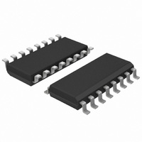
PCA9633D16,112 NXP Semiconductors, PCA9633D16,112 Datasheet - Page 21

PCA9633D16,112
Manufacturer Part Number
PCA9633D16,112
Description
IC LED DRIVER RGBA 16-SOIC
Manufacturer
NXP Semiconductors
Type
RGBA LED Driverr
Datasheet
1.PCA9633DP2118.pdf
(43 pages)
Specifications of PCA9633D16,112
Package / Case
16-SOIC (3.9mm Width)
Topology
Open Drain, PWM
Number Of Outputs
4
Internal Driver
Yes
Type - Primary
Backlight, LED Blinker
Type - Secondary
RGBA
Frequency
1MHz
Voltage - Supply
2.3 V ~ 5.5 V
Voltage - Output
5.5V
Mounting Type
Surface Mount
Operating Temperature
-40°C ~ 85°C
Current - Output / Channel
25mA
Internal Switch(s)
Yes
Low Level Output Current
17 mA
High Level Output Current
50 uA
Operating Supply Voltage
2.3 V to 5.5 V
Maximum Supply Current
100 mA
Maximum Power Dissipation
400 mW
Maximum Operating Temperature
+ 85 C
Mounting Style
SMD/SMT
Minimum Operating Temperature
- 40 C
Operating Supply Voltage (typ)
2.5/3.3/5V
Number Of Segments
8
Operating Temperature (min)
-40C
Operating Temperature (max)
85C
Operating Temperature Classification
Industrial
Package Type
SO
Pin Count
16
Mounting
Surface Mount
Power Dissipation
400mW
Operating Supply Voltage (min)
2.3V
Operating Supply Voltage (max)
5.5V
Lead Free Status / RoHS Status
Lead free / RoHS Compliant
For Use With
OM6282 - DAUGHTER CARD PCA9633 FOR OM6275OM6276,598 - DEMO BOARD PWM LED622-1004 - BOARD DEMO FOR PHILIPS PCA9633
Efficiency
-
Lead Free Status / Rohs Status
Lead free / RoHS Compliant
Other names
568-3235-5
935281309112
PCA9633D16
935281309112
PCA9633D16
NXP Semiconductors
8. Characteristics of the I
PCA9633_5
Product data sheet
8.1.1 START and STOP conditions
8.1 Bit transfer
8.2 System configuration
The I
lines are a serial data line (SDA) and a serial clock line (SCL). Both lines must be
connected to a positive supply via a pull-up resistor when connected to the output stages
of a device. Data transfer may be initiated only when the bus is not busy.
One data bit is transferred during each clock pulse. The data on the SDA line must remain
stable during the HIGH period of the clock pulse as changes in the data line at this time
will be interpreted as control signals (see
Both data and clock lines remain HIGH when the bus is not busy. A HIGH-to-LOW
transition of the data line while the clock is HIGH is defined as the START condition (S). A
LOW-to-HIGH transition of the data line while the clock is HIGH is defined as the STOP
condition (P) (see
A device generating a message is a ‘transmitter’; a device receiving is the ‘receiver’. The
device that controls the message is the ‘master’ and the devices which are controlled by
the master are the ‘slaves’ (see
Fig 12. Bit transfer
Fig 13. Definition of START and STOP conditions
2
C-bus is for 2-way, 2-line communication between different ICs or modules. The two
SDA
SCL
START condition
2
SDA
SCL
Figure
C-bus
S
Rev. 05 — 25 July 2008
13).
Figure
data valid
data line
stable;
14).
Figure
allowed
change
of data
12).
4-bit Fm+ I
STOP condition
mba607
P
PCA9633
2
© NXP B.V. 2008. All rights reserved.
C-bus LED driver
mba608
SDA
SCL
21 of 43


