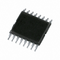
PCA9922PW,112 NXP Semiconductors, PCA9922PW,112 Datasheet - Page 6

PCA9922PW,112
Manufacturer Part Number
PCA9922PW,112
Description
IC LED DRIVER 8-CH 16-TSSOP
Manufacturer
NXP Semiconductors
Type
Linear (Serial Interface)r
Datasheet
1.PCA9922PW112.pdf
(27 pages)
Specifications of PCA9922PW,112
Constant Current
Yes
Number Of Outputs
8
Internal Driver
Yes
Type - Primary
General Purpose
Type - Secondary
Color
Frequency
25MHz
Voltage - Supply
3.3 V ~ 5.5 V
Voltage - Output
5.5V
Mounting Type
Surface Mount
Package / Case
16-TSSOP
Operating Temperature
-40°C ~ 85°C
Current - Output / Channel
60mA
Internal Switch(s)
Yes
Lead Free Status / RoHS Status
Lead free / RoHS Compliant
Efficiency
-
Topology
-
Lead Free Status / Rohs Status
Details
Other names
935285711112
NXP Semiconductors
7. Functional description
PCA9922
Product data sheet
7.1 System interface
The PCA9922 is an 8-channel constant current LED driver with built-in LED output error
detection. The PCA9922 contains an 8-bit shift register and data latches, which convert
serial input data into parallel output data.
At the output stage, 8 regulated current sinks are designed to provide constant and
uniform current through LEDs with different forward voltages (V
Refer to
During normal operation, serial data can be transferred into the PCA9922 through SDI,
shifted into the shift register, and out through the SDO. Data shifts from the SDI pin into
the next sequential bit in the shift register on each rising edge of the CLK input. The MSB
is the first bit to be clocked in. Data shifts out of the shift register and is presented on the
SDO pin on the falling edge of CLK. The exception to this is during the error detect
sequence, at which time the error status is loaded in a parallel fashion into the shift
register. The shift register is never disabled. It is either shifting or it is loading the error
status on every rising edge of CLK. Additionally, the device is designed such that it may
be cascaded with other similar devices. The SDO pin contains the output of the shift
register which may be used for cascading to the SDI pin of the next device in the series.
Data is parallel loaded from the serial shift register to an output control register when LE
(Latch Enable) is asserted HIGH (serial-to-parallel conversion). The output control register
will continue to reflect the shift register data, even if changes occur in the shift register
data, as long as LE is HIGH. When LE is LOW the latch is closed and changes in the shift
register data no longer effect the output control register. Applications where the latches
are bypassed (LE tied HIGH) will require that the OE input be HIGH during serial data
entry.
The data in the output control register is then used to drive the constant current output
drivers when the outputs are enabled. The outputs are globally enabled or disabled
through the OE. A LOW level on the OE will enable the output drivers, LED0 to LED7, to
reflect the data contained in the output control register.
An example timing diagram of expected normal operation of the device is shown in
Figure
Remark: It is recommended that OE and LE pulse widths be at least two clocks wide
when CLK is running to avoid inadvertent entry into the error detect modes.
There is no synchronization logic in the design between CLK, LE and OE. It is the user’s
responsibility to meet the timing presented in
operation.
5.
Figure 1 “Block diagram of
All information provided in this document is subject to legal disclaimers.
8-channel constant current LED driver with output error detection
Rev. 2 — 6 April 2011
PCA9922”.
Table 10
in order to guarantee proper
F
).
PCA9922
© NXP B.V. 2011. All rights reserved.
6 of 27


