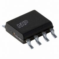
PCA9553D/01,118 NXP Semiconductors, PCA9553D/01,118 Datasheet - Page 5

PCA9553D/01,118
Manufacturer Part Number
PCA9553D/01,118
Description
IC LED DRIVER LINEAR 8-SOIC
Manufacturer
NXP Semiconductors
Type
Linear (I²C Interface)r
Datasheet
1.PCA9553DP01118.pdf
(26 pages)
Specifications of PCA9553D/01,118
Package / Case
8-SOIC (3.9mm Width)
Topology
Open Drain, PWM
Number Of Outputs
4
Internal Driver
Yes
Type - Primary
LED Blinker
Frequency
400kHz
Voltage - Supply
2.3 V ~ 5.5 V
Mounting Type
Surface Mount
Operating Temperature
-40°C ~ 85°C
Current - Output / Channel
25mA
Internal Switch(s)
Yes
Low Level Output Current
25 mA
Operating Supply Voltage
2.3 v to 5.5 V
Maximum Supply Current
500 uA
Maximum Power Dissipation
400 mW
Maximum Operating Temperature
+ 85 C
Mounting Style
SMD/SMT
Minimum Operating Temperature
- 40 C
Lead Free Status / RoHS Status
Lead free / RoHS Compliant
Voltage - Output
-
Efficiency
-
Lead Free Status / Rohs Status
Lead free / RoHS Compliant
Other names
935272825118
PCA9553D/01-T
PCA9553D/01-T
PCA9553D/01-T
PCA9553D/01-T
NXP Semiconductors
7. Functional description
PCA9553_6
Product data sheet
7.1 Device address
7.2 Control register
Refer to
Following a START condition the bus master must output the address of the slave it is
accessing. The address of the PCA9553/01 is shown in
Figure
PCA9553TK uses the version /01 address.
The last bit of the address byte defines the operation to be performed. When set to logic 1
a read is selected, while a logic 0 selects a write operation.
Following the successful acknowledgement of the slave address, the bus master will send
a byte to the PCA9553 which will be stored in the Control register.
The lowest 3 bits are used as a pointer to determine which register will be accessed.
If the Auto-Increment flag is set, the three low order bits of the Control register are
automatically incremented after a read or write. This allows the user to program the
registers sequentially. The contents of these bits will rollover to ‘000’ after the last register
is accessed.
When the Auto-Increment flag is set (AI = 1) and a read sequence is initiated, the
sequence must start by reading a register different from ‘0’ (B2 B1 B0
Only the 3 least significant bits are affected by the AI flag.
Unused bits must be programmed with zeroes.
Fig 5.
Fig 7.
6.
1
Figure 1 “Block
PCA9553/01 slave address
Reset state: 00h
Control register
1
slave address
0
0
Rev. 06 — 29 December 2008
0
diagram”.
1
4-bit I
002aad742
0
0
Auto-Increment
R/W
0
2
C-bus LED driver with programmable blink rates
0
flag
AI
Fig 6.
0
register address
B2
002aad744
1
B1
PCA9553/02 slave address
Figure 5
1
B0
slave address
0
0
and PCA9553/02 in
0
PCA9553
© NXP B.V. 2008. All rights reserved.
0 0 0).
1
002aad743
1
R/W
5 of 26


