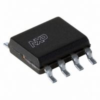
PCA9553D/01,118 NXP Semiconductors, PCA9553D/01,118 Datasheet - Page 8

PCA9553D/01,118
Manufacturer Part Number
PCA9553D/01,118
Description
IC LED DRIVER LINEAR 8-SOIC
Manufacturer
NXP Semiconductors
Type
Linear (I²C Interface)r
Datasheet
1.PCA9553DP01118.pdf
(26 pages)
Specifications of PCA9553D/01,118
Package / Case
8-SOIC (3.9mm Width)
Topology
Open Drain, PWM
Number Of Outputs
4
Internal Driver
Yes
Type - Primary
LED Blinker
Frequency
400kHz
Voltage - Supply
2.3 V ~ 5.5 V
Mounting Type
Surface Mount
Operating Temperature
-40°C ~ 85°C
Current - Output / Channel
25mA
Internal Switch(s)
Yes
Low Level Output Current
25 mA
Operating Supply Voltage
2.3 v to 5.5 V
Maximum Supply Current
500 uA
Maximum Power Dissipation
400 mW
Maximum Operating Temperature
+ 85 C
Mounting Style
SMD/SMT
Minimum Operating Temperature
- 40 C
Lead Free Status / RoHS Status
Lead free / RoHS Compliant
Voltage - Output
-
Efficiency
-
Lead Free Status / Rohs Status
Lead free / RoHS Compliant
Other names
935272825118
PCA9553D/01-T
PCA9553D/01-T
PCA9553D/01-T
PCA9553D/01-T
NXP Semiconductors
8. Characteristics of the I
PCA9553_6
Product data sheet
8.1.1 START and STOP conditions
7.4 Pins used as general purpose I/Os
7.5 Power-on reset
8.1 Bit transfer
LED pins not used to control LEDs can be used as general purpose I/Os.
For use as input: Set LEDn to high-impedance (01) and then read the pin state via the
Input register.
For use as output: Connect external pull-up resistor to the pin and size it according to the
DC recommended operating characteristics. LED output pin is HIGH when the output is
programmed as high-impedance, and LOW when the output is programmed LOW through
the ‘LED selector’ register. The output can be pulse-width controlled when PWM0 or
PWM1 are used.
When power is applied to V
a reset condition until V
and the PCA9553 registers are initialized to their default states, with all outputs in the OFF
state. Thereafter, V
The I
lines are a serial data line (SDA) and a serial clock line (SCL). Both lines must be
connected to a positive supply via a pull-up resistor when connected to the output stages
of a device. Data transfer may be initiated only when the bus is not busy.
One data bit is transferred during each clock pulse. The data on the SDA line must remain
stable during the HIGH period of the clock pulse as changes in the data line at this time
will be interpreted as control signals (see
Both data and clock lines remain HIGH when the bus is not busy. A HIGH-to-LOW
transition of the data line while the clock is HIGH is defined as the START condition (S). A
LOW-to-HIGH transition of the data line while the clock is HIGH is defined as the STOP
condition (P) (see
Fig 8.
2
C-bus is for 2-way, 2-line communication between different ICs or modules. The two
Bit transfer
2
SDA
SCL
Figure
C-bus
DD
Rev. 06 — 29 December 2008
must be lowered below 0.2 V to reset the device.
DD
9).
has reached V
DD
, an internal Power-On Reset (POR) holds the PCA9553 in
4-bit I
data valid
data line
stable;
2
C-bus LED driver with programmable blink rates
POR
Figure
. At that point, the reset condition is released
allowed
change
of data
8).
mba607
PCA9553
© NXP B.V. 2008. All rights reserved.
8 of 26


