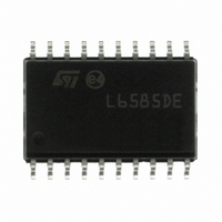
L6585DETR STMicroelectronics, L6585DETR Datasheet - Page 16

L6585DETR
Manufacturer Part Number
L6585DETR
Description
IC PFC/BALLAST CONTROL 20-SOIC
Manufacturer
STMicroelectronics
Type
PFC/Ballast Controllerr
Datasheet
1.L6585DETR.pdf
(33 pages)
Specifications of L6585DETR
Frequency
58.4 ~ 62 kHz
Current - Supply
7mA
Current - Output
600mA
Voltage - Supply
11 V ~ 16 V
Operating Temperature
-40°C ~ 150°C
Package / Case
20-SOIC (7.5mm Width)
Switching Frequency
250 KHz
Maximum Power Dissipation
830 mW
Maximum Operating Temperature
+ 150 C
Mounting Style
SMD/SMT
Minimum Operating Temperature
- 40 C
Lead Free Status / RoHS Status
Lead free / RoHS Compliant
Other names
497-8822-2
Available stocks
Company
Part Number
Manufacturer
Quantity
Price
Company:
Part Number:
L6585DETR
Manufacturer:
STMicroelectronics
Quantity:
1 792
Part Number:
L6585DETR
Manufacturer:
ST
Quantity:
20 000
Application information
5.2.2
5.2.3
16/33
The ZCD input can be connected directly to an auxiliary winding of the PFC choke in order
to turn on the MOSFET when the choke current reaches zero. This pin has internal clamps
and high current capability that makes it compliant with a very wide range of input voltage.
At startup, when PFC choke is not yet energized, an internal starter gives ZCD pulses to the
PFC gate driver with a repetition rate of approximately 15 kHz.
By turning off the MOSFET when the current reaches the threshold and turning on the
MOSFET when the choke current reaches zero, a triangular input current whose peaks are
modulated by the MULT voltage is obtained. By feeding the MULT pin with the mains
waveform, a power factor correction and THD reduction is achieved.
Leading edge blanking
Usually current sense voltage is filtered by means of an RC network in order to avoid false
turning off of the MOSFET because of the discharge current related to parasitic drain
capacitance present at the beginning of the on time of the MOSFET. This filtering generates
a delay between the actual threshold crossing and the input triggering. During this time the
PFC inductor current increases and the choke may saturate. A leading edge blanking
structure makes the PFCCS input active only after 200 ns (typ.) after the PFG turn on. This
allows the use of inductors with lower saturation current. However, if saturation occurs, a
choke saturation protection turns off the PFC gate as soon as the voltage at pin PFCCS is
above 1.7 V.
Figure 6.
THD optimizer feature
When the input voltage passes through zero, the PFC choke cannot store energy because
of the very low voltage across it. This may cause heavy crossover distortion and subsequent
THD degradation. A small offset voltage superimposed over the MULT voltage can reduce
this issue.
The internal THD optimizer increases the performance when the mains voltage reaches
zero; this reduces crossover distortion and avoids offset introduction.
PFCCS waveforms
L6585DE


