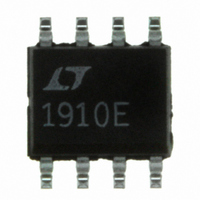
LT1910ES8#PBF Linear Technology, LT1910ES8#PBF Datasheet - Page 10

LT1910ES8#PBF
Manufacturer Part Number
LT1910ES8#PBF
Description
IC MOSFET DRIVER HIGH-SIDE 8SOIC
Manufacturer
Linear Technology
Datasheet
1.LT1910ES8PBF.pdf
(12 pages)
Specifications of LT1910ES8#PBF
Configuration
High-Side
Input Type
Non-Inverting
Delay Time
220µs
Number Of Configurations
1
Number Of Outputs
1
Voltage - Supply
8 V ~ 48 V
Operating Temperature
-40°C ~ 85°C
Mounting Type
Surface Mount
Package / Case
8-SOIC (3.9mm Width)
Lead Free Status / RoHS Status
Lead free / RoHS Compliant
Current - Peak
-
High Side Voltage - Max (bootstrap)
-
Available stocks
Company
Part Number
Manufacturer
Quantity
Price
LT1910
APPLICATIONS INFORMATION
Low Voltage/Wide Supply Range Operation
When the supply is less than 12V, the LT1910’s charge
pump does not produce suffi cient gate voltage to fully
enhance the standard N-channel MOSFET. For these ap-
plications, a logic-level MOSFET can be used to extend
the operating supply down to 8V. If the MOSFET has a
maximum V
can also operate up to a supply voltage of 60V (absolute
maximum rating of the V
Protecting Against Supply Transients
The LT1910 is 100% tested and guaranteed to be safe
from damage with 60V applied between the V
pins. However, when this voltage is exceeded, even for a
few microseconds, the result can be catastrophic. For this
reason it is imperative that the LT1910 is not exposed to
supply transients above 60V. A transient suppressor, such
as Diodes Inc.’s SMAJ48A, should be added between the
V
For proper current sense operation, the V
to be connected to the positive side of the drain-sense
resistor (see Drain-Sense Confi guration). Therefore, the
supply should be adequately decoupled at the node where
the V
microfarads may be required when operating with a high
current switch.
When the operating voltage approaches the 60V absolute
maximum rating of the LT1910, local supply decoupling
10
+
and GND pins for such applications.
+
pin and drain sense resistor meet. Several hundred
GS
rating of 15V or greater, then the LT1910
FAULT OUTPUT
+
pin).
INPUT
5V
Figure 8b. Low Side Driver for Source Current Sensing
R1
5.1k
+
3
4
2
pin is required
C
1μF
FAULT
IN
TIMER
T
+
LT1910
GND
and GND
SENSE
1
GATE
V
10μF
+
50V
C1
8V TO 24V
8
6
5
+
2N2222
between the V
RC snubber with a transient suppressor are an absolute
necessity. Note however that resistance should not be
added in series with the V
error in the current-sense threshold.
Low Side Driving
Although the LT1910 is primarily targeted at high side
(grounded load) switch applications, it can also be used
for low side (supply connected load) switch applications.
Figures 8a and 8b illustrate the LT1910 driving low side
power MOSFETs. Because the LT1910 charge pump tries
to pump the gate of the N-channel MOSFET above the
supply, a clamp Zener is required to prevent the V
solute maximum) of the MOSFET from being exceeded.
FAULT OUTPUT
51Ω
51Ω
Figure 8a. Low Side Driver with Load Current Sensing
12V TO 48V
INPUT
LT1006
5V
0V
1N4744
+
and GND pins is highly recommended. An
15V
+
–
R1
5.1k
2
3
4
C
1μF
1910 F08b
FAULT
IN
TIMER
T
LOAD
HV
HV
LT1910
GND
+
Q1
IRF630
R
0.02Ω
SENSE
S
1
pin because it will cause an
GATE
V
+
8
6
5
+
C1
100μF
100V
15V
1N4744
LOAD
4A
1910 F08a
Q1
IRFZ44
R
0.01Ω
(PTC)
S
GS
(ab-
1910fa


