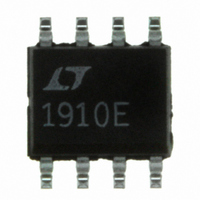
LT1910ES8#PBF Linear Technology, LT1910ES8#PBF Datasheet - Page 8

LT1910ES8#PBF
Manufacturer Part Number
LT1910ES8#PBF
Description
IC MOSFET DRIVER HIGH-SIDE 8SOIC
Manufacturer
Linear Technology
Datasheet
1.LT1910ES8PBF.pdf
(12 pages)
Specifications of LT1910ES8#PBF
Configuration
High-Side
Input Type
Non-Inverting
Delay Time
220µs
Number Of Configurations
1
Number Of Outputs
1
Voltage - Supply
8 V ~ 48 V
Operating Temperature
-40°C ~ 85°C
Mounting Type
Surface Mount
Package / Case
8-SOIC (3.9mm Width)
Lead Free Status / RoHS Status
Lead free / RoHS Compliant
Current - Peak
-
High Side Voltage - Max (bootstrap)
-
Available stocks
Company
Part Number
Manufacturer
Quantity
Price
LT1910
APPLICATIONS INFORMATION
to the supply at the same point as the positive end of the
sense resistor.
The drain-sense threshold voltage has a positive tempera-
ture coeffi cient, allowing PTC sense resistors to be used
(see Printed Circuit Board Shunts). The selection of R
should be based on the minimum threshold voltage:
Thus the 0.02Ω drain-sense resistor in Figure 3 will yield
a minimum trip current of 2.5A. This simple confi guration
is appropriate for resistive or inductive loads that do not
generate large current transients at turn-on.
Automatic Restart Period
The timing capacitor, C
the length of time the power MOSFET is held off follow-
ing a current limit trip. Curves are given in the Typical
Performance Characteristics to show the restart period
for various values of C
a 50ms restart period.
Defeating Automatic Restart
Some applications are required to remain off after a fault
occurs. When the LT1910 is being driven from CMOS logic,
this can be easily implemented by connecting resistor R2
between the IN and TIMER pins as shown in Figure 4. R2
supplies the sustaining current for an internal SCR which
latches the TIMER pin LOW under a fault condition. The
FAULT pin is set active LOW when the TIMER pin falls below
3.3V. This keeps the MOSFET gate from turning on and the
8
R
Figure 4. Latch-Off Confi guration (Autorestart Defeated)
S
= 50mV/I
CMOS
LOGIC
5V
SET
ON = 5V
OFF = 0V
FAULT OUTPUT
T
T
. For example, C
, shown in Figure 3 determines
5V
R2
2k
R1
5.1k
3
4
2
C
1μF
T
FAULT
IN
TIMER
LT1910
GND
T
= 0.33μF yields
1
1910 F04
S
FAULT pin from resetting HIGH until the IN pin has been
recycled. C
ing whenever the IN pin recycles to turn on the MOSFET
unsuccessfully under an existing fault condition.
Inductive vs Capacitive Loads
Turning on an inductive load produces a relatively benign
ramp in MOSFET current. However, when an inductive
load is turned off, the current stored in the inductor needs
somewhere to decay. A clamp diode connected directly
across each inductive load normally serves this purpose.
If a diode is not employed, the LT1910 clamps the MOSFET
gate 0.7V below ground. This causes the MOSFET to resume
conduction during the current decay with (V
across it, resulting in high dissipation peaks.
Capacitive loads exhibit the opposite behavior. Any load
that includes a decoupling capacitor will generate a current
equal to C
large electrolytic capacitors, the resulting current spike
can play havoc with the power supply and false trip the
current-sense comparator.
Turn-on ∂V/∂t is controlled by the addition of the simple
network shown in Figure 5. This network takes advantage of
the fact that the MOSFET acts as a source follower during
turn-on. Thus the ∂V/∂t on the source can be controlled
by controlling the ∂V/∂t on the gate.
LT1910
GND
Figure 5. Control and Current Limit Delay
LOAD
T
SENSE
1
is used to prevent the FAULT pin from glitch-
GATE
50μF
V
50V
C2
+
• (∂V/∂t) during capacitor in-rush. With
8
6
5
+
∂V/∂t CONTROL NETWORK
DELAY NETWORK
CURRENT LIMIT
100k
R1
C
1N4148
D
R
1N4148
D
100k
(≤10k)
C1
R2
+
+
24V
+ V
R
0.01Ω
Q1
IRFZ34
15V
1N4744
S
GS
C
1910 F05
LOAD
+ 0.7V)
1910fa


