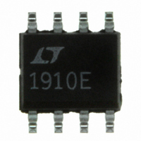
LT1910ES8#PBF Linear Technology, LT1910ES8#PBF Datasheet - Page 7

LT1910ES8#PBF
Manufacturer Part Number
LT1910ES8#PBF
Description
IC MOSFET DRIVER HIGH-SIDE 8SOIC
Manufacturer
Linear Technology
Datasheet
1.LT1910ES8PBF.pdf
(12 pages)
Specifications of LT1910ES8#PBF
Configuration
High-Side
Input Type
Non-Inverting
Delay Time
220µs
Number Of Configurations
1
Number Of Outputs
1
Voltage - Supply
8 V ~ 48 V
Operating Temperature
-40°C ~ 85°C
Mounting Type
Surface Mount
Package / Case
8-SOIC (3.9mm Width)
Lead Free Status / RoHS Status
Lead free / RoHS Compliant
Current - Peak
-
High Side Voltage - Max (bootstrap)
-
Available stocks
Company
Part Number
Manufacturer
Quantity
Price
OPERATION
also activates the open-collector NPN to pull the FAULT
pin LOW, indicating an overcurrent condition.
When the MOSFET gate voltage is discharged to less than
1.4V, the TIMER pin is released. The 14μA current source
then slowly charges the timing capacitor back to 2.9V
where the charge pump again starts to drive the GATE pin
HIGH. If a fault condition still exists, the sense comparator
threshold will again be exceeded and the timer cycle will
repeat until the fault is removed. The FAULT pin becomes
inactive HIGH if the TIMER pin charges up successfully
above 3.4V (see Figure 1).
APPLICATIONS INFORMATION
Input/Supply Sequencing
There are no input/supply sequencing requirements for
the LT1910. The IN pin may be taken up to 15V with the
supply at 0V. When the supply is turned on with the IN pin
set HIGH, the MOSFET turn-on will be inhibited until the
timing capacitor charges up to 2.9V (i.e., for one restart
cycle).
Isolating the Inputs
Operation in harsh environments may require isolation to
prevent ground transients from damaging control logic.
The LT1910 easily interfaces to low cost optoisolators. The
network shown in Figure 2 ensures that the input will be
pulled above 2V, but not exceed the absolute maximum
rating for supply voltages of 12V to 48V over the entire
LOGIC
INPUT
LOGIC GROUND
2k
Figure 2. Isolating the Input
12V TO 48V
100k
51k
4
POWER GROUND
IN
LT1910
GND
1
1910 F02
temperature range. The optoisolator must have less than
20μA of dark current (leakage) at hot in order to maintain
the off state (see Figure 2).
Drain-Sense Confi guration
The LT1910 uses supply referenced current sensing. One
input of the current-sense comparator is connected to a
drain-sense pin, while the second input is offset 65mV
below the supply inside the device. For this reason, Pin 8
of the LT1910 must be treated not only as a supply pin,
but also as the reference input for the current-sense
comparator.
Figure 3 shows the proper drain-sense confi guration for
the LT1910. Note that the SENSE pin goes to the drain
end of the sense resistor, while the V
FAULT OUTPUT
TIMER
FAULT
GATE
IN
INPUT
3.5V
2.9V
24V
0V
0V
0V
5V
0V
V
5V
0V
+
Figure 3. Drain-Sense Confi guration
12V
OFF
R1
5.1k
Figure 1. Timing Diagram
NORMAL
3
4
2
C
1μF
FAULT
IN
TIMER
T
LT1910
GND
SENSE
1
GATE
OVERCURRENT
V
+
8
6
5
+
C1
100μF
50V
+
pin is connected
LT1910
3.4V
1910 F03
NORMAL
Q1
IRFZ34
R
0.02Ω
(PTC)
S
24V
2A
SOLENOID
1910 F01
1910fa
7


