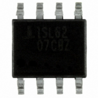
ISL6207CBZ Intersil, ISL6207CBZ Datasheet - Page 7

ISL6207CBZ
Manufacturer Part Number
ISL6207CBZ
Description
IC DRIVER MOSFET DUAL SYNC 8SOIC
Manufacturer
Intersil
Datasheet
1.ISL6207CBZ.pdf
(10 pages)
Specifications of ISL6207CBZ
Configuration
High and Low Side, Synchronous
Input Type
PWM
Delay Time
20ns
Current - Peak
2A
Number Of Configurations
1
Number Of Outputs
2
High Side Voltage - Max (bootstrap)
36V
Voltage - Supply
4.5 V ~ 5.5 V
Operating Temperature
-10°C ~ 85°C
Mounting Type
Surface Mount
Package / Case
8-SOIC (3.9mm Width)
Lead Free Status / RoHS Status
Lead free / RoHS Compliant
The next larger standard value capacitance is 0.22µF. A
good quality ceramic capacitor is recommended.
Power Dissipation
Package power dissipation is mainly a function of the
switching frequency and total gate charge of the selected
MOSFETs. Calculating the power dissipation in the driver for
a desired application is critical to ensuring safe operation.
Exceeding the maximum allowable power dissipation level
will push the IC beyond the maximum recommended
operating junction temperature of 125°C. The maximum
allowable IC power dissipation for the SO-8 package is
approximately 800mW. When designing the driver into an
application, it is recommended that the following calculation
be performed to ensure safe operation at the desired
frequency for the selected MOSFETs. The power dissipated
by the driver is approximated as:
where f
and V
and Q
MOSFET selection and any external capacitance added to
the gate pins. The I
of the driver and is typically negligible.
P
=
FIGURE 2. BOOTSTRAP CAPACITANCE vs BOOT RIPPLE
f
sw
L
L
2.0
1.8
1.6
1.4
1.2
1.0
0.8
0.6
0.4
0.2
0.0
sw
(
represent the upper and lower gate rail voltage. Q
is the upper and lower gate charge determined by
1.5V
0.0
is the switching frequency of the PWM signal. V
U
20nC
VOLTAGE
0.1
Q
U
+
0.2
V
DDQ
50nC
L
Q
Q
GATE
0.3
L
V
)
+
CC
= 100nC
I
DDQ
0.4
product is the quiescent power
∆V
7
BOOT
V
0.5
CC
(V)
0.6
0.7
0.8
0.9
1.0
U
U
ISL6207
Layout Considerations
Reducing Phase Ring
The parasitic inductances of the PCB and power devices
(both upper and lower FETs) could cause increased PHASE
ringing, which may lead to voltages that exceed the absolute
maximum rating of the devices. When PHASE rings below
ground, the negative voltage could add charge to the
bootstrap capacitor through the internal bootstrap diode.
Under worst-case conditions, the added charge could
overstress the BOOT and/or PHASE pins. To prevent this
from happening, the user should perform a careful layout
inspection to reduce trace inductances, and select low lead
inductance MOSFETs and drivers. D
packaged MOSFETs have high parasitic lead inductances, as
opposed to SOIC-8. If higher inductance MOSFETs must be
used, a Schottky diode is recommended across the lower
MOSFET to clamp negative PHASE ring.
A good layout would help reduce the ringing on the phase
and gate nodes significantly:
• Avoid using vias for decoupling components where
• All power traces (UGATE, PHASE, LGATE, GND, VCC)
• Keep the SOURCE of the upper FET as close as thermally
• Keep the connection in between the SOURCE of lower
• Input capacitors should be placed as close to the DRAIN
possible, especially in the BOOT-to-PHASE path. Little or
no use of vias for VCC and GND is also recommended.
Decoupling loops should be short.
should be short and wide, and avoid using vias. If vias
must be used, two or more vias per layer transition is
recommended.
possible to the DRAIN of the lower FET.
FET and power ground wide and short.
of the upper FET and the SOURCE of the lower FET as
thermally possible.
1000
900
800
700
600
500
400
300
200
100
FIGURE 3. POWER DISSIPATION vs FREQUENCY
0
0
Q
Q
200
U
L
=200nC
=100nC
400
600
Q
Q
FREQUENCY (kHz)
L
U
=100nC
=50nC
800
1000 1200 1400 1600 1800 2000
2
PAK and DPAK
Q
Q
U
L
=50nC
=50nC
December 2, 2005
Q
Q
U
L
=50nC
=20nC
FN9075.8


