IRS26302DJPBF International Rectifier, IRS26302DJPBF Datasheet
IRS26302DJPBF
Specifications of IRS26302DJPBF
Available stocks


Related parts for IRS26302DJPBF

IRS26302DJPBF Summary of contents
Page 1
... Motor control • Typical Connection Diagram www.irf.com FULLY PROTECTED 3-PHASE BRIDGE PLUS ONE GATE Product Summary Topology V OFFSET V OUT I & I (typical Deadtime (typical) Package June 2009 IRS26302DJPBF DRIVER 3 Phase 600 – 200 mA & 350 mA 290 ns 44-Lead PLCC © 2009 International Rectifier ...
Page 2
... Dynamic Electrical Characteristics Functional Block Diagram Input/Output Pin Equivalent Circuit Diagram Lead Definitions Lead Assignments Application Information and Additional Details Parameter Temperature Trends Package Details Tape and Reel Details Part Marking Information Ordering Information www.irf.com © 2009 International Rectifier 2 IRS26302DJ Page ...
Page 3
... Description The IRS26302DJPBF are high voltage, high speed power MOSFET and IGBT drivers with three independent high and low side referenced output channels for 3-phase applications. An additional low side driver is included for PFC or Brake IGBT driving operation. Proprietary HVIC technology enables rugged monolithic construction. Logic inputs are compatible with CMOS or LSTTL outputs, down to 3 ...
Page 4
... Typical Application Diagram www.irf.com V cc VDC GF VSDC HIN (x3) LIN (x3 FLT/EN PCFin/BRin PCFout/BRout PCFtrip/BRtrip RCIN ITRIP COM IRS26302DJ © 2009 International Rectifier ...
Page 5
... Charged Device Model IC Latch-Up Test RoHS Compliant † Qualification standards can be found at International Rectifier’s web site †† Higher qualification ratings may be available should the user have such requirements. Please contact your International Rectifier sales representative for further information. ††† Higher MSL ratings may be available for the specific package types listed here. ...
Page 6
... Min. Max. Units -0.3 620 0.3 S1,2,3 B1,2 0.3 B1,2,3 B 1,2,3 -0.3 620 VDC-20 VDC+0.3 VDC-20 VDC+0.3 † 0 0.3 CC — 50 V/ns — 4.6 — 27 ° C/W — 150 -55 150 — 300 © 2009 International Rectifier V W ° C ...
Page 7
... V with pulse width. Guaranteed by design. Refer IRS26302DJ Min. Max S1,2,3 S1,2 S1,2,3 B1,2,3 Vss – 8 600 -50 600 (TBD) 600 VDC-5 VDC VDC-12 VDC- - S1,2,3 B1,2,3 COM -40 125 of – –V . Please refer to Design Tip S BS © 2009 International Rectifier Units V ºC ...
Page 8
... V — 12.0 11.8 — VB1,2,3 = VDC = GF =600 V, 50 µA VDC - VDCS = 20 V 120 All input/output in off status 4 mA All input/output in off status — Vout = </= 10 us — mA Vout = </= 0.6 © 2009 International Rectifier and ...
Page 9
... V, PW </= 10 us FCOUT </= 10 us — FCOUT 1400 600 860 ITRIP ITRIP µA V =-250 mV — PFCTRIP PFCTRIP RCIN 3.3V EN 100 I = 1.5 mA 100 I = 1.5 mA — VDC - Vgf = 250 mV, 300 VDC -600 V µA 300 VDC = Vgf , VDC + = 40- 600 V © 2009 International Rectifier and ...
Page 10
... V FCIN — 2.2 nF LOAD — 2.2 nF LOAD 650 3 — ITRIP 3 600 ITRIP — — — & 3 — LIN = 3 HIN = 0 V 420 3 input = 100 680 pF µs RCIN 600 FLT/En = ITRIP 1500 ns 3 LOx/Hox = ITRIP 950 © 2009 International Rectifier 3 ...
Page 11
... BRTRIP 850 -1 FCOUT 750 1800 FLT/ 1300 LOx/Hox = 1200 FCOUT 550 3.3 V, LINx/HINx EN 500 = 3 LOx/Hox = 3 LINx/HINx EN 560 = 3 LOx/Hox = 3 500 3 FCIN RIN FCOUT ROUT 500 3 FCIN RIN P /B =15 V FCOUT ROUT See fault diagnostic state 700 diagram = © 2009 International Rectifier ...
Page 12
... UV detect Noise filter HV Fault and level Diagnostic shifter Logic latch Noise filter FAULT REGISTER Noise filter 12 IRS26302DJ Driver Driver V B2 HO2 Driver LO2 Driver COM HO3 Driver V S3 LO3 Driver Driver PFCout/ BRout DCS ITRIP PFCtrip/ BRtrip © 2009 International Rectifier ...
Page 13
... Input/Output Pin Equivalent Circuit www.irf.com Diagrams 13 IRS26302DJ © 2009 International Rectifier ...
Page 14
... Description , then automatically becomes inactive (open-drain high impedance). FLTCLR /B becomes inactive, FAULT stays active low for an FCTRIP/ RTRIP , then automatically becomes inactive (open-drain high impedance). FLTCLR , then automatically becomes inactive (open-drain high impedance). FLTCLR 14 IRS26302DJ ) approximately FLTCLR © 2009 International Rectifier ...
Page 15
... Lead Assignments www.irf.com © 2009 International Rectifier 15 IRS26302DJ ...
Page 16
... OUT Figure 1: HVIC sourcing current www.irf.com . The voltage that drives the gate of the external power switch is defined as O for the low-side power switch; this parameter is sometimes generically LO Figure 2: HVIC sinking current 16 IRS26302DJ © 2009 International Rectifier ...
Page 17
... IC has received a command from the control IC to shutdown); this results in the outputs (HOx and LOx) being held in the low state until the enable pin is pulled high. www.irf.com Figure 3: Switching time waveforms 17 IRS26302DJ , and t ) associated IN OUT ON OFF R F © 2009 International Rectifier RCIN,TH ...
Page 18
... IRS26302DJ specifies the maximum difference between DT comparing the DT of one channel of the IRS26302DJ to that of another. www.irf.com Figure 4: Input/output timing diagram Figure 5: Detailed view of B & C intervals and IRS26302DJ . The MDT parameter also applies when 2 © 2009 International Rectifier ...
Page 19
... V and 5 V logic-level signals. Figure 8 illustrates an input signal to the IRS26302DJ, its input threshold values, and the logic state of the result of the input signal. www.irf.com Figure 7: Illustration of deadtime ) of the IRS26302DJ is matched to the propagation turn-on delay ON Figure 8: HIN & LIN input thresholds 19 IRS26302DJ , t ) for both the low-side ON OFF © 2009 International Rectifier ...
Page 20
... CCUV- threshold, the IC will not turn-on. Additionally, if the V BSUV threshold during operation, the undervoltage lockout circuitry will recognize a fault Figure 9: UVLO protection 20 IRS26302DJ (logic and low-side circuitry) power supply CC ( plotted over the undervoltage protection is enabled or BSUV+/- © 2009 International Rectifier BS ...
Page 21
... Table 2 gives a summary of this pin’s functionality and EN Enable Input Enable input high Outputs enabled Enable input low Outputs disabled Table 2: Enable functionality truth table (*assumes no other fault condition) 21 IRS26302DJ Please refer to the EN pin FILTER,EN * © 2009 International Rectifier ...
Page 22
... SS and the RCIN pin, while C CC Figure 13: Programming the fault clear timer C 1 nF, ceramic RCIN 0 RCIN >> R Table 3: Design guidelines 22 IRS26302DJ is placed between the RCIN RCIN ON,RCIN © 2009 International Rectifier or ITRIP, CC ...
Page 23
... IT,TH /( IT,TH could The voltage of the ITRIP pin should not be allowed IRS26302DJ / The circuit designer will need to IT,TH and R such that the voltage and the temperature changes, the 4 . The resistor values should X © 2009 International Rectifier , ...
Page 24
... ITRIP functionality by the time that IT,TH+ temperature protection has been tripped; the CC is not latched in this case and CCUV RCIN FAULT LO HO High High High Z LIN 0 High High Z LIN HIN Low Low Low High High © 2009 International Rectifier and PCFout 0 0 PCFIN ...
Page 25
... Reset DIAG MODE: hold Linx=H Hinx=L www.irf.com Condi RCIN Itrip PFCtrip tion Fault register = 1 (**) 0 V > Vth (**) X (*) 0 V > Vth (**) X (*) > Vth (**) (*) > Vth (**) (*) > Vth (**) (*) > Vth (**) (*) (*) (*) Figure 17: State Diagram 25 IRS26302DJ GF VCC fault EN/FLT Lox V > 0-> < < > © 2009 International Rectifier PFCout/ Hox BRout ...
Page 26
... Figure 18: Fault Query Procedure 26 IRS26302DJ © 2009 International Rectifier ...
Page 27
... FIL,IN FIL,IN Figure 21: Noise rejecting input filters 27 IRS26302DJ ; the resulting output is approximately the FIL,IN ; the resulting output is FIL,IN Figure 20: Advanced input filter ; the output does not change states. Example 2 of © 2009 International Rectifier ; the FIL,IN ...
Page 28
... ON and narrow OFF cases is shown in OUT IN –PW duration. This data illustrates the performance and near symmetry OUT IN Figure 22: IRS2336xD input filter characteristic 28 IRS26302DJ duration. It can be seen that for a PW OUT durations mimic the PW durations very well over IN © 2009 International Rectifier ...
Page 29
... Design Tip 04-4 (DT04-4) entitled “Using Monolithic High Voltage Gate Drivers.” This design tip is available at www.irf.com. www.irf.com , see Figure 24 for an illustration of this internal connection Figure 25: Bootstrap MOSFET state diagram 29 IRS26302DJ CC voltage is higher than approximately 110% B returns below that threshold; this B © 2009 International Rectifier supply and ...
Page 30
... COM pins and how these two grounds are used in the system. The SS -COM; the gate-emitter voltage ( G, Figure 26: Separate V and COM pins SS 30 IRS26302DJ in the figure is the voltage between the the low-side switch is the swings from the positive DC bus S1 © 2009 International Rectifier ...
Page 31
... PCB tracks are lumped together in L www.irf.com Figure 27: Three phase inverter Figure 29: D2 conducting Figure 31: Q4 conducting voltage swing does not stop at the level of the negative DC bus, rather it S and L for each IGBT. When the high-side switch is on IRS26302DJ , S2 transient”. S © 2009 International Rectifier ...
Page 32
... International Rectifier’s HVICs have been designed for the robustness required in many of today’s demanding applications. The IRS26302DJ has been seen to withstand large negative V V for a period of 50 ns. An illustration of the IRS26302DJ’ ...
Page 33
... Supply Capacitor recommended to place a bypass capacitor (C connection is shown in Figure 37. component should be placed as close as possible to the pins in order to reduce parasitic elements. www.irf.com Figure 36: Antenna Loops A ceramic 1 F ceramic capacitor is suitable for most applications. This Figure 37: Supply capacitor 33 IRS26302DJ ) between the V and V pins. This © 2009 International Rectifier ...
Page 34
... AN-1123: Bootstrap Network Analysis: Focusing on the Integrated Bootstrap Functionality DT04-4: Using Monolithic High Voltage Gate Drivers AN-978: HV Floating MOS-Gate Driver ICs www.irf.com spikes remain excessive, further steps S or less) between the V and V (see Figure 39). See DT04 Figure 39: V clamping diode S © 2009 International Rectifier 34 IRS26302DJ pin and the switch S ...
Page 35
... IRS26302DJ 0.35 0.30 0.25 0.20 0.15 0.10 Exp. 0.05 0.00 -50 - Temperature ( C) Fig. 41. Input Bias Current vs. Temperature 0.05 0.04 0.03 0.02 Exp. 0.01 0.00 -0.01 -50 - Temperature ( C) Fig. 43. RCIN Input Bias Current vs. Temperature © 2009 International Rectifier 100 125 100 125 ...
Page 36
... Fig. 45. PFC Input Bias Current TRIP vs. Temperature 2.00 1.60 1.20 Exp. 0.80 0.40 0.00 -50 - Temperature ( C) Fig. 47. ITRIP Input Bias Current vs. Temperature 100 80 60 Exp -50 - Temperature ( C) Fig. 49. Quiescent V Supply Current BS vs. Temperature © 2009 International Rectifier 75 100 125 75 100 125 100 125 ...
Page 37
... Exp. 600 400 200 0 -50 - Temperature ( C) Fig. 51. Turn-Off Propagation Delay vs. Temperature Exp -50 - Temperature ( C) Fig. 53. Turn-Off Fall Time vs. Temperature 1000 800 Exp. 600 400 200 0 -50 - Temperature ( C) Fig. 55. Turn-Off Propagation Delay vs. Temperature © 2009 International Rectifier 100 125 100 125 100 125 ...
Page 38
... C) 38 IRS26302DJ Exp -50 - Temperature ( C) Fig. 57. Turn-Off Fall Time vs. Temperature 1000 800 600 Exp. 400 200 0 -50 - Temperature ( C) Fig. 59. Turn-Off Propagation Delay vs. Temperature 100 80 60 Exp -50 - Temperature ( C) Fig. 61. Turn-Off Fall Time vs. Temperature © 2009 International Rectifier 100 125 100 125 100 125 ...
Page 39
... C) 39 IRS26302DJ Exp -50 - Temperature ( C) Fig. 63. Ton, Off Matching Time vs. Temperature Exp -50 - Temperature ( C) Fig. 65. Pulse Width Distortion vs. Temperature 2000 1600 Exp. 1200 800 400 0 -50 - Temperature ( C) Fig. 67. ITRIP to Fault Time vs. Temperature © 2009 International Rectifier 100 125 100 125 75 100 125 ...
Page 40
... Temperature ( C) Shutdown Propagation OUT Delay vs. Temperature 800 600 Exp. 400 200 0 -50 - Temperature ( C) 800 600 Exp. 400 200 0 -50 - Temperature ( C) Fig. 73. PFC to Output Shutdown TRIP Propagation Delay vs. Temperature © 2009 International Rectifier 100 125 100 125 100 125 ...
Page 41
... Temperature ( C) Fig. 75. FAULT Clear Time RCIN vs. Temperature 2500 2000 Exp. 1500 1000 500 0 -50 - Temperature ( C) Fig. 77 Fault Time TRIP vs. Temperature Exp. 500 0 -50 - Temperature ( C) Fig. 79 PFC Output Shutdown TRIP Propagation Delay vs. © 2009 International Rectifier 100 125 100 125 100 125 ...
Page 42
... Temperature ( C) vs. Temperature 500 400 300 Exp. 200 100 0 -50 - Temperature ( C) Fig. 83. Enable Input Filter Time vs. Temperature Exp. 0 -50 - Temperature ( C) Fig. 85. EN off to Output Shutdown PFC Propagation Delay vs. Temperature © 2009 International Rectifier 100 125 100 125 100 125 ...
Page 43
... Temperature 1000 800 600 400 Exp. 200 0 -50 - Temperature ( C) Fig. 89. Output High Short Circuit Pulsed Current PFC vs. Temperature OUT Exp. 0 -50 - Temperature ( C) Fig. 91. Output Low Short Circuit Pulsed Current, HO1,2,3 vs. Temperature © 2009 International Rectifier 100 125 100 125 100 125 ...
Page 44
... IRS26302DJ Exp. 0 -50 - Temperature ( o C) Fig. 93. RCIN Low On Resistance vs. Temperature Exp. -50 - Temperature (oC) Fig. 95. Input Negative Going Threshold vs. Temperature Exp. -50 - Temperature (oC) Fig. 97. Input Negative Going Threshold vs. Temperature © 2009 International Rectifier 100 125 100 125 100 125 ...
Page 45
... Fig. 101. GF Negative Going Threshold 15.00 12.00 9.00 6.00 3.00 0.00 75 100 125 Fig. 103. RCIN Positive Going Threshold vs. 45 IRS26302DJ Exp. -50 - Temperature (oC) vs. Temperature Exp. -50 - Temperature (oC) vs. Temperature Exp. -50 - Temperature (oC) Temperature © 2009 International Rectifier 100 125 100 125 100 125 ...
Page 46
... Fig. 109 IRS26302DJ Exp. -50 - Temperature (oC) Supply Undervoltage Positive CC Going Threshold vs. Temperature Exp. -50 - Temperature (oC) Fig. 107. V Supply Undervoltage BS Hysteresis vs. Temperature Exp. -50 - Temperature (oC) Supply Undervoltage Positive BS Going Threshold vs. Temperature © 2009 International Rectifier 100 125 100 125 100 125 ...
Page 47
... Fig. 113. High Level Output Voltage 0.05 0.04 0.03 0.02 0.01 0.00 75 100 125 47 IRS26302DJ Exp. -50 - Temperature (oC PFC vs. Temperature O OUT Exp. 0.00 -50 - Temperature (oC HO1,2,3 vs. Temperature O Exp. -50 - Temperature ( C) Fig. 115. En Input Bias Current vs. Temperature © 2009 International Rectifier 100 125 - BIAS 100 125 - BIAS 100 125 ...
Page 48
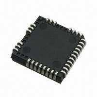
... Package Details: PLCC44 www.irf.com © 2009 International Rectifier 48 IRS26302DJ ...
Page 49
... E 98.00 102.00 3.858 F n/a 38.4 n/a G 34.7 35.8 1.366 H 32.6 33.1 1.283 49 IRS26302DJ Imperial Max 0.948 0.161 1.271 0.562 0.712 0.712 n/a 0.062 D A Imperial Max 13.001 0.844 0.519 0.096 4.015 1.511 1.409 1.303 © 2009 International Rectifier ...
Page 50
... Part Marking Information www.irf.com © 2009 International Rectifier 50 IRS26302DJ ...
Page 51
... For technical support, please contact IR’s Technical Assistance Center www.irf.com Standard Pack Form Quantity Tube/Bulk Tape and Reel 500 http://www.irf.com/technical-info/ WORLD HEADQUARTERS: 233 Kansas St., El Segundo, California 90245 Tel: (310) 252-7105 51 IRS26302DJ Complete Part Number 27 IRS26302DJPBF IRS26302DJTRPBF © 2009 International Rectifier ...