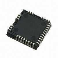
IRS26302DJPBF International Rectifier, IRS26302DJPBF Datasheet - Page 31

IRS26302DJPBF
Manufacturer Part Number
IRS26302DJPBF
Description
IC BRIDGE +1 GATE DVR 3PH 44PLCC
Manufacturer
International Rectifier
Datasheet
1.IRS26302DJTRPBF.pdf
(51 pages)
Specifications of IRS26302DJPBF
Configuration
3 Phase Bridge
Input Type
Non-Inverting
Delay Time
320ns
Current - Peak
200mA
Number Of Configurations
1
Number Of Outputs
3
High Side Voltage - Max (bootstrap)
600V
Voltage - Supply
10 V ~ 20 V
Operating Temperature
-40°C ~ 125°C
Mounting Type
Surface Mount
Package / Case
44-PLCC (32 Leads)
Number Of Drivers
6
Driver Configuration
Non-Inverting
Driver Type
High and Low Side
Input Logic Level
CMOS/TTL
Rise Time
190ns
Fall Time
75ns
Propagation Delay Time
710ns
Peak Output Current
350mA
Power Dissipation
4.6W
Operating Supply Voltage (min)
10V
Turn Off Delay Time
50ns
Turn On Delay Time (max)
50ns
Operating Temp Range
-40C to 125C
Operating Temperature Classification
Automotive
Mounting
Surface Mount
Pin Count
32
Package Type
PLCC
Lead Free Status / RoHS Status
Lead free / RoHS Compliant
Available stocks
Company
Part Number
Manufacturer
Quantity
Price
Company:
Part Number:
IRS26302DJPBF
Manufacturer:
International Rectifier
Quantity:
10 000
IRS26302DJ
Figure 27: Three phase inverter
Figure 28: Q1 conducting
Figure 29: D2 conducting
Also when the V phase current flows from the inductive load back to the inverter (see Figures 30 and 31), and Q4
IGBT switches on, the current commutation occurs from D3 to Q4. At the same instance, the voltage node, V
,
S2
swings from the positive DC bus voltage to the negative DC bus voltage.
Figure 30: D3 conducting
Figure 31: Q4 conducting
However, in a real inverter circuit, the V
voltage swing does not stop at the level of the negative DC bus, rather it
S
swings below the level of the negative DC bus. This undershoot voltage is called “negative V
transient”.
S
The circuit shown in Figure 32 depicts one leg of the three phase inverter; Figures 33 and 34 show a simplified
illustration of the commutation of the current between Q1 and D2. The parasitic inductances in the power circuit from
the die bonding to the PCB tracks are lumped together in L
and L
for each IGBT. When the high-side switch is on,
C
E
www.irf.com
© 2009 International Rectifier
31


