IRS26302DJPBF International Rectifier, IRS26302DJPBF Datasheet - Page 16
IRS26302DJPBF
Manufacturer Part Number
IRS26302DJPBF
Description
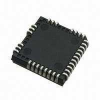
IC BRIDGE +1 GATE DVR 3PH 44PLCC
Manufacturer
International Rectifier
Datasheet
1.IRS26302DJTRPBF.pdf
(51 pages)
Specifications of IRS26302DJPBF
Configuration
3 Phase Bridge
Input Type
Non-Inverting
Delay Time
320ns
Current - Peak
200mA
Number Of Configurations
1
Number Of Outputs
3
High Side Voltage - Max (bootstrap)
600V
Voltage - Supply
10 V ~ 20 V
Operating Temperature
-40°C ~ 125°C
Mounting Type
Surface Mount
Package / Case
44-PLCC (32 Leads)
Number Of Drivers
6
Driver Configuration
Non-Inverting
Driver Type
High and Low Side
Input Logic Level
CMOS/TTL
Rise Time
190ns
Fall Time
75ns
Propagation Delay Time
710ns
Peak Output Current
350mA
Power Dissipation
4.6W
Operating Supply Voltage (min)
10V
Turn Off Delay Time
50ns
Turn On Delay Time (max)
50ns
Operating Temp Range
-40C to 125C
Operating Temperature Classification
Automotive
Mounting
Surface Mount
Pin Count
32
Package Type
PLCC
Lead Free Status / RoHS Status
Lead free / RoHS Compliant
Available stocks
Company
Part Number
Manufacturer
Quantity
Price
Company:

Part Number:
IRS26302DJPBF
Manufacturer:
International Rectifier
Quantity:
10 000


Application Information and Additional Details
Information regarding the following topics are included as subsections within this section of the datasheet.
IGBT/MOSFET Gate Drive
The IRS26302DJ HVICs are designed to drive MOSFET or IGBT power devices. Figures 1 and 2 illustrate several
parameters associated with the gate drive functionality of the HVIC. The output current of the HVIC, used to drive the
gate of the power switch, is defined as I
V
called V
www.irf.com
HO
•
•
•
•
•
•
•
•
•
•
•
•
•
•
•
•
•
•
•
•
•
for the high-side power switch and V
OUT
IGBT/MOSFET Gate Drive
Switching and Timing Relationships
Deadtime
Matched Propagation Delays
Input Logic Compatibility
Undervoltage Lockout Protection
Shoot-Through Protection
Enable Input
Fault Reporting and Programmable Fault Clear Timer
Over-Current Protection
Over-Temperature Shutdown Protection
Truth Table: Undervoltage lockout, ITRIP, and ENABLE
Diagnostics
Advanced Input Filter
Short-Pulse / Noise Rejection
Integrated Bootstrap Functionality
Bootstrap Power Supply Design
Separate Logic and Power Grounds
Tolerant to Negative V
PCB Layout Tips
Additional Documentation
and in this case does not differentiate between the high-side or low-side output voltage.
Figure 1: HVIC sourcing current
S
Transients
O
. The voltage that drives the gate of the external power switch is defined as
LO
for the low-side power switch; this parameter is sometimes generically
16
Figure 2: HVIC sinking current
© 2009 International Rectifier
IRS26302DJ
Related parts for IRS26302DJPBF
Image
Part Number
Description
Manufacturer
Datasheet
Request
R

Part Number:
Description:
SCHOTTKY RECTIFIER
Manufacturer:
International Rectifier Corp.
Datasheet:
Part Number:
Description:
SCHOTTKY RECTIFIER
Manufacturer:
International Rectifier Corp.
Datasheet:
Part Number:
Description:
SCHOTTKY RECTIFIER
Manufacturer:
International Rectifier Corp.
Datasheet:
Part Number:
Description:
SCHOTTKY RECTIFIER
Manufacturer:
International Rectifier Corp.
Datasheet:
Part Number:
Description:
SCHOTTKY RECTIFIER
Manufacturer:
International Rectifier Corp.
Datasheet:
Part Number:
Description:
SCHOTTKY RECTIFIER
Manufacturer:
International Rectifier Corp.
Datasheet:
Part Number:
Description:
SCHOTTKY RECTIFIER
Manufacturer:
International Rectifier Corp.
Datasheet:
Part Number:
Description:
SCHOTTKY RECTIFIER
Manufacturer:
International Rectifier Corp.
Datasheet:
Part Number:
Description:
SCHOTTKY RECTIFIER
Manufacturer:
International Rectifier Corp.
Datasheet:
Part Number:
Description:
SCHOTTKY RECTIFIER
Manufacturer:
International Rectifier Corp.
Datasheet:
Part Number:
Description:
SCHOTTKY RECTIFIER
Manufacturer:
International Rectifier Corp.
Datasheet:
Part Number:
Description:
SCHOTTKY RECTIFIER
Manufacturer:
International Rectifier Corp.
Datasheet:
Part Number:
Description:
SCHOTTKY RECTIFIER
Manufacturer:
International Rectifier Corp.
Datasheet:
Part Number:
Description:
SCHOTTKY RECTIFIER
Manufacturer:
International Rectifier Corp.
Datasheet:
Part Number:
Description:
SCHOTTKY RECTIFIER
Manufacturer:
International Rectifier Corp.
Datasheet: