ISL6700IR Intersil, ISL6700IR Datasheet
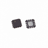
IC DRIVER HALF BRIDGE DUAL 12QFN

ISL6700IR

Manufacturer Part Number
ISL6700IR
Description
IC DRIVER HALF BRIDGE DUAL 12QFN
Manufacturer
Intersil
Datasheet

Specifications of ISL6700IR

Configuration
Half Bridge
Input Type
PWM
Delay Time
70ns
Current - Peak
1.4A
Number Of Configurations
1
Number Of Outputs
2
High Side Voltage - Max (bootstrap)
80V
Voltage - Supply
9 V ~ 15 V
Operating Temperature
-40°C ~ 125°C
Mounting Type
Surface Mount
Package / Case
12-QFN
Lead Free Status / RoHS Status
Contains lead / RoHS non-compliant

Available stocks

Company
Part Number
Manufacturer
Quantity
Price
Company:
Part Number:
ISL6700IR
Quantity:
107
80V/1.25A Peak, Medium Frequency, Low
Cost, Half-Bridge Driver
The ISL6700 is an 80V/1.25A peak, medium frequency, low
cost, half-bridge driver IC available in 8-lead SOIC and
12-lead QFN plastic packages. The low-side and high-side
gate drivers are independently controlled and matched to
25ns. This gives the user maximum flexibility in dead-time
selection and driver protocol. Undervoltage protection on
both the low-side and high-side supplies force the outputs
low. Non-latching, level-shift translation is used to control the
upper drive circuit. Unlike some competitors, the high-side
output returns to its correct state after a momentary
undervoltage of the high-side supply.
Ordering Information
Pinouts
ISL6700IB
ISL6700IBZ
(See Note)
ISL6700IR
ISL6700IRZ
(See Note)
Add “-T” suffix to part number for tape and reel packaging.
NOTE: Intersil Pb-free products employ special Pb-free material
sets; molding compounds/die attach materials and 100% matte tin
plate termination finish, which are RoHS compliant and compatible
with both SnPb and Pb-free soldering operations. Intersil Pb-free
products are MSL classified at Pb-free peak reflow temperatures that
meet or exceed the Pb-free requirements of IPC/JEDEC J STD-020.
NUMBER
PART
TEMP. RANGE
V
V
-40 to 125
-40 to 125
-40 to 125
-40 to 125
DD
SS
HI
LI
(°C)
ISL6700IB (SOIC)
1
2
3
4
TOP VIEW
®
1
8 Ld SOIC
8 Ld SOIC
(Pb-free)
12 Ld 4x4 QFN
12 Ld 4x4 QFN
(Pb-free)
PACKAGE
Data Sheet
8
7
6
5
HB
HO
HS
LO
M8.15
M8.15
L12.4x4
L12.4x4
PKG. DWG. #
1-888-INTERSIL or 321-724-7143
CAUTION: These devices are sensitive to electrostatic discharge; follow proper IC Handling Procedures.
Features
• Drives 2 N-Channel MOSFETs in Half-Bridge
• Space Saving SO8 and Low R
• Phase Supply Max Voltage to 80VDC
• Bootstrap Supply Max Voltage to 96VDC
• Drives 1000pF Load with Rise and Fall Times Typ. 15ns
• TTL/CMOS Compatible Input Thresholds
• Independent Inputs for Non-Half-Bridge Topologies
• No Start-Up Problems
• Low Power Consumption
• Wide Supply Range
• Supply Undervoltage Protection
• QFN Package
• Pb-Free Available (RoHS Compliant)
Applications
• Telecom/Datacom Power Supplies
• Half-Bridge Converters
• Two-Switch Forward Converters
• Active Clamp Forward Converters
December 29, 2004
Configuration
- Compliant to JEDEC PUB95 MO-220 QFN
- Quad Flat No Leads - Package Outline
All other trademarks mentioned are the property of their respective owners.
|
Intersil (and design) is a registered trademark of Intersil Americas Inc.
Copyright © Intersil Americas Inc. 2002-2004. All Rights Reserved.
NC
NOTE: EPAD = Exposed PAD.
HI
LI
1
2
3
ISL6700IR (QFN)
12
4
TOP VIEW
EPAD
11
5
C-S
10
6
QFN Packages
9
8
7
HO
NC
HS
ISL6700
FN9077.6

Related parts for ISL6700IR

ISL6700IR Summary of contents

Page 1

... Two-Switch Forward Converters • Active Clamp Forward Converters CAUTION: These devices are sensitive to electrostatic discharge; follow proper IC Handling Procedures. | 1-888-INTERSIL or 321-724-7143 All other trademarks mentioned are the property of their respective owners. ISL6700 FN9077.6 QFN Packages C-S ISL6700IR (QFN) TOP VIEW EPAD ...

Page 2

Application Block Diagram PWM CONTROLLER Functional Block Diagram ISL6700 +12V DRIVE DRIVE LI LO ISL6700 V SS U/V DETECTOR UNDERVOLTAGE EPAD (QFN PACKAGE ONLY) +48V ...

Page 3

ISL6700 +12V ISL6700 PWM FIGURE 1. TWO-SWITCH FORWARD CONVERTER +12V ISL6700 PWM FIGURE 2. FORWARD CONVERTER WITH AN ACTIVE CLAMP 3 +48V SECONDARY CIRCUIT ISOLATION +48V SECONDARY CIRCUIT ISOLATION FN9077.6 December 29, 2004 ...

Page 4

Absolute Maximum Ratings Supply Voltage, V (Note -0.3V to 16V DD LI and HI Voltages (Note ...

Page 5

Electrical Specifications PARAMETERS GATE DRIVER OUTPUT PINS: LO & HO Low Level Output Voltage High Level Output Voltage Peak Pullup Current Peak Pulldown Current Switching Specifications PARAMETERS Lower Turn-off Propagation Delay (LI ...

Page 6

Timing Diagrams HI HPLH t LPLH HO, LO FIGURE 3. 6 ISL6700 HPHL LO t LPHL MON MOFF FIGURE 4. FN9077.6 December 29, 2004 ...

Page 7

... Dimensions D2 and E2 are for the exposed pads which provide improved electrical and thermal performance. 8. Nominal dimensions are provided to assist with PCB Land Pattern Design efforts, see Intersil Technical Brief TB389. 9. Features and dimensions A2, A3, D1, E1, P & θ are present when Anvil singulation method is used and not present for saw singulation ...

Page 8

... Accordingly, the reader is cautioned to verify that data sheets are current before placing orders. Information furnished by Intersil is believed to be accurate and reliable. However, no responsibility is assumed by Intersil or its subsidiaries for its use; nor for any infringements of patents or other rights of third parties which may result from its use ...

Related keywords