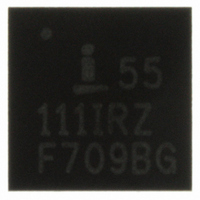
ISL55111IRZ Intersil, ISL55111IRZ Datasheet - Page 13

ISL55111IRZ
Manufacturer Part Number
ISL55111IRZ
Description
IC MOSFET DRIVER DUAL HS 16-QFN
Manufacturer
Intersil
Type
High Sider
Datasheet
1.ISL55110IRZ.pdf
(15 pages)
Specifications of ISL55111IRZ
Input Type
Non-Inverting
Number Of Outputs
2
On-state Resistance
3 Ohm
Current - Output / Channel
300mA
Current - Peak Output
3.5A
Voltage - Supply
5 V ~ 13.2 V
Operating Temperature
-40°C ~ 85°C
Mounting Type
Surface Mount
Package / Case
16-VQFN Exposed Pad, 16-HVQFN, 16-SQFN, 16-DHVQFN
Lead Free Status / RoHS Status
Lead free / RoHS Compliant
Power Dissipation Discussion
Specifying continuous pulse rates, driver loads and driver
level amplitudes are key in determining power supply
requirements, as well as dissipation/cooling necessities.
Driver Output patterns also impact these needs. The faster
the pin activity, the greater the need to supply current and
remove heat.
As detailed in the “Power Dissipation Calculation” on
page 12, Power Dissipation of the device is calculated by
taking the DC current of the V
(Driver rail) times the respective voltages and adding the
product of both calculations. The average DC current
measurements of I
the device with the planned V
the required pulse activity of both channels at the desired
operating frequency and driver loads.
Therefore, the user must address power dissipation relative
to the planned operating conditions. Even with a device
mounted per Notes 4 or 5 under Thermal Information, given
the high speed pulse rate and amplitude capability of the
ISL55110, ISL55111, it is possible to exceed the +150°C
“absolute-maximum junction temperature”. Therefore, it is
important to calculate the maximum junction temperature for
the application to determine if operating conditions need to
be modified for the device to remain in the safe operating
area.
The maximum power dissipation allowed in a package is
determined according to Equation 2:
where:
• T
• T
• θ
• P
Intersil products are sold by description only. Intersil Corporation reserves the right to make changes in circuit design, software and/or specifications at any time without
notice. Accordingly, the reader is cautioned to verify that data sheets are current before placing orders. Information furnished by Intersil is believed to be accurate and
reliable. However, no responsibility is assumed by Intersil or its subsidiaries for its use; nor for any infringements of patents or other rights of third parties which may result
from its use. No license is granted by implication or otherwise under any patent or patent rights of Intersil or its subsidiaries.
P
2. 10pF is the approximate parasitic Capacitor (Inverters,
3. 135pF is the approximate parasitic at the D
4. C
DMAX
AMAX
JA
JMAX
DMAX
channel power consumption, only include this current
once.
etc.), which the V
Buffers. This includes the effect of the Crow-bar Current.
L
= Thermal resistance of the package
is the Load capacitor being driven
=
= Maximum junction temperature
= Maximum ambient temperature
T
-------------------------------------------- -
= Maximum power dissipation in the package
JMAX
All Intersil U.S. products are manufactured, assembled and tested utilizing ISO9000 quality systems.
θ
JA
- T
DD
Intersil Corporation’s quality certifications can be viewed at www.intersil.com/design/quality
AMAX
DD
and IH should be done while running
For information regarding Intersil Corporation and its products, see www.intersil.com
drives
13
DD
DD
and V
(logic) and V
H
levels and driving
H
OUT
Current
ISL55110, ISL55111
and its
(EQ. 2)
The maximum power dissipation actually produced by an IC
is the total quiescent supply current times the total power
supply voltage, plus the power in the IC due to the loads.
Power also depends on number of channels changing state
and frequency of operation. The extent of continuous active
pulse generation will greatly effect dissipation requirements.
The user should evaluate various heat sink/cooling options
in order to control the ambient temperature part of the
equation. This is especially true if the user’s applications
require continuous, high speed operation. A review of the
θ
the QFN package to have better thermal characteristics.
The reader is cautioned against assuming a calculated
level of thermal performance in actual applications. A
careful inspection of conditions in your application
should be conducted. Great care must be taken to
ensure Die Temperature does not exceed +
Absolute Maximum Thermal Limits.
Important Note: The ISL55110, ISL55111 QFN package
metal plane is used for heat sinking of the device. It is
electrically connected to the negative supply potential
ground.
Power Supply Sequencing
Apply V
Power Up Considerations
Digital Inputs should never be open. Do not apply slow
analog ramps to the inputs. Again, place decoupling as close
to the package as possible for both V
Special Loading
With most applications, the user will usually have a special
load requirement. Please contact Intersil for Evaluation
Boards or to request a device characterization to your
requirements in our lab.
.
JA
ratings of the TSSOP and QFN package clearly show
DD
, then V
H
.
DD
and especially V
150°C
March 17, 2011
FN6228.4
H
.


