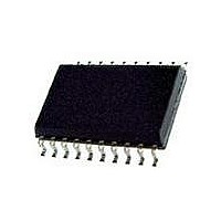
L6201PS STMicroelectronics, L6201PS Datasheet

L6201PS
Specifications of L6201PS
Available stocks
Related parts for L6201PS
L6201PS Summary of contents
Page 1
... SUPPLY VOLTAGE UP TO 48V 5A MAX PEAK CURRENT (2A max. for L6201) TOTAL RMS CURRENT UP TO L6201: 1A; L6202: 1.5A; L6203/L6201PS 0.3 (typical value (ON) CROSS CONDUCTION PROTECTION TTL COMPATIBLE DRIVE OPERATING FREQUENCY UP TO 100 KHz THERMAL SHUTDOWN INTERNAL LOGIC SUPPLY HIGH EFFICIENCY DESCRIPTION The I ...
Page 2
L6201 - L6202 - L6203 PIN CONNECTIONS (Top view) SO20 GND OUT2 OUT1 BOOT1 GND 2/20 1 N. IN1 8 N. D95IN216 PowerSO20 MULTIWATT11 POWERDIP 20 GND 19 N.C. ...
Page 3
... V Boostrap Peak Voltage b P Total Power Dissipation: tot for L6201 pins for L6202 for L6201PS/L6203 case for L6201 (Note 2) amb for L6202 (Note 2) for L6201PS/L6203 (Note Storage and Junction Temperature stg j Note 1: Pulse width limited only by junction temperature and transient thermal impedance (see thermal characteristics) Note 2: Mounted on board with minimized dissipating copper area ...
Page 4
... Test Conditions I = 2mA REF Fig. 1,2,3) Fig Fig. 4,5 Fig L6201 1.2A L6202 DS L6201PS Fig. 6a and L6201 1.2A L6202 L6201PS/ dif = L6201 1.2A L6202 L6203 Unit L6202 L6203 12 – – 42V unless S sens Min. Typ. Max. Unit 13.5 ...
Page 5
ELECTRICAL CHARACTERISTICS (Continued) LOGIC CONTROL TO POWER DRIVE TIMING Symbol Parameter Source Current Turn-off Delay Source Current Fall Time Source Current Turn-on Delay ...
Page 6
... L6201 - L6202 - L6203 Figure 5: Normalized R DS (ON) Figure 6a: Typical Diode Behaviour in Synchro- nous Rectification (L6201) Figure 7a: Typical Power Dissipation vs I (L6201) 6/ vs. Temperature Typical Values Figure 6b: Typical Diode Behaviour in Synchro- Figure 7b: Typical Power Dissipation nous Rectification (L6201PS/02/03) L (L6201PS, L6202, L6203)) ...
Page 7
Figure 8a: Two Phase Chopping Figure 8b: One Phase Chopping Figure 8c: Enable Chopping L6201 - L6202 - L6203 IN1 = 7/20 ...
Page 8
L6201 - L6202 - L6203 TEST CIRCUITS Figure 9: Saturation Voltage Figure 10: Quiescent Current Figure 11: Leakage Current 8/20 ...
Page 9
... Figure 12: Source Current Delay Times vs. Input Chopper 42V for Figure 13: Sink Current Delay Times vs. Input Chopper 42V for L6201PS/02/03 L6201PS/02/03 L6201 - L6202 - L6203 9/20 ...
Page 10
L6201 - L6202 - L6203 CIRCUIT DESCRIPTION The L6201/1PS/2 monolithic full bridge switching motor driver realized in the new Mul- tipower-BCD technology which allows the integra- tion of multiple, isolated DMOS power transistors plus mixed CMOS/bipolar control circuits. ...
Page 11
Boostrap Capacitors To ensure that the POWER DMOS transistors are driven correctly gate to source voltage of typ must be guaranteed for all of the N-channel DMOS transistors. This is easy to be provided for the lower POWER ...
Page 12
L6201 - L6202 - L6203 Quiescent Energy The last contribution to the energy dissipation is due to the quiescent supply current and is given by QUIESCENT QUIESCENT Total Energy Per Cycle TOT ...
Page 13
... R2) to establish the comparator refer- ence voltage and a snubber network made by R and C in series (See DC Motor Speed Control). L6201 L6201PS L6202 L6203 L6201 L6201PS L6202 L6203 L6201 L6201PS L6202 L6203 L6201 L6201PS L6202 L6203 13/20 ...
Page 14
... Supply Voltage value, may be a good solu- tion the one shown in Fig. 20. Figure 20: L6201/1P/2/3 Used at a Supply Volt- age Range Between 9 and 18V L6201 L6201PS L6202 L6203 THERMAL CHARACTERISTICS Thanks to the high efficiency of this device, often a true heatsink is not needed simply ob- tained by means of a copper side on the P ...
Page 15
Figure 24: Typical Transient Thermal Resistance for Single Pulses (L6202) Figure 26: Typical Transient Thermal Resistance for Single Pulses with and without Heatsink (L6203) L6201 - L6202 - L6203 Figure 25: Typical R of Multiwatt Th J-amb Package vs. Total ...
Page 16
L6201 - L6202 - L6203 mm DIM. MIN. TYP. MAX. a1 0.51 B 0.85 1.40 b 0.50 b1 0.38 0.50 D 24.80 E 8.80 e 2.54 e3 20.32 F 7.10 I 5.10 L 3.30 Z 2.54 16/20 inch MIN. TYP. ...
Page 17
DIM. MIN. TYP. MAX. MIN. A 2.35 2.65 0.093 A1 0.1 0.3 0.004 B 0.33 0.51 0.013 C 0.23 0.32 0.009 D 12.6 13 0.496 E 7.4 7.6 0.291 e 1. 10.65 0.394 h 0.25 0.75 0.010 ...
Page 18
L6201 - L6202 - L6203 mm DIM. MIN. TYP. MAX. A 3.6 a1 0.1 0.3 0.004 a2 3 0.1 0.000 b 0.4 0.53 0.016 c 0.23 0.32 0.009 D (1) 15.8 16 0.622 D1 9.4 9.8 0.370 E ...
Page 19
DIM. MIN. TYP. MAX. MIN 2. 0.49 0.55 0.019 F 0.88 0.95 0.035 G 1.45 1.7 1.95 0.057 G1 16.75 17 17.25 0.659 H1 19.6 0.772 H2 20.2 L 21.9 22.2 ...
Page 20
... This publication supersedes and replaces all information previously supplied. STMicroelectronics products are not authorized for use as critical components in life support devices or systems without express written approval of STMicroelectronics. © 2003 STMicroelectronics – Printed in Italy – All Rights Reserved Australia - Brazil - Canada - China - Finland - France - Germany - Hong Kong - India - Israel - Italy - Japan - Malaysia - Malta - Morocco - Singapore - Spain - Sweden - Switzerland - United Kingdom - United States ...


