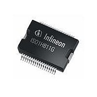
ISO1H811G Infineon Technologies, ISO1H811G Datasheet - Page 4

ISO1H811G
Manufacturer Part Number
ISO1H811G
Description
IC SWITCH HISIDE 8CH DSO-36
Manufacturer
Infineon Technologies
Type
High Sider
Series
ISOFACE™r
Datasheet
1.ISO1H811G.pdf
(20 pages)
Specifications of ISO1H811G
Package / Case
DSO-36
Input Type
Non-Inverting
Number Of Outputs
8
On-state Resistance
150 mOhm
Current - Output / Channel
700mA
Current - Peak Output
1.4A
Voltage - Supply
11 V ~ 35 V
Operating Temperature
-25°C ~ 125°C
Mounting Type
Surface Mount
Product
Driver ICs - Various
Propagation Delay Time
10 ns
Supply Voltage (max)
6.5 V
Supply Voltage (min)
- 0.5 V
Maximum Power Dissipation
3.3 W
Maximum Operating Temperature
Internally Limited
Mounting Style
SMD/SMT
Minimum Operating Temperature
- 25 C
Lead Free Status / RoHS Status
Lead free / RoHS Compliant
Lead Free Status / RoHS Status
Lead free / RoHS Compliant, Lead free / RoHS Compliant
Other names
SP000413798
Available stocks
Company
Part Number
Manufacturer
Quantity
Price
Part Number:
ISO1H811G
Manufacturer:
INFINEON/英飞凌
Quantity:
20 000
Company:
Part Number:
ISO1H811GAUMA1
Manufacturer:
TI
Quantity:
1 400
1
1.1
Pin
Datasheet
TAB
10
11
12
13
14
15
16
17
18
19
20
21
22
23
24
25
26
27
28
29
30
31
32
33
34
35
36
1
2
3
4
5
6
7
8
9
Symbol
GNDCC
GNDbb
OUT7
OUT7
OUT6
OUT6
OUT5
OUT5
OUT4
OUT4
OUT3
OUT3
OUT2
OUT2
OUT1
OUT1
OUT0
OUT0
DIAG
VCC
N.C.
N.C.
N.C.
N.C.
N.C
Vbb
DIS
WR
CS
D0
D1
D2
D3
D4
D5
D6
D7
Pin Configuration and Functionality
Pin Configuration
Function
Not connected
Positive 3.3/5V logic supply
Output disable
Chip select
Parallel write
Data input bit0
Data input bit1
Data input bit2
Data input bit3
Data input bit4
Data input bit5
Data input bit6
Data input bit7
Common diagnostic output for
overtemperature
Input logic ground
Not connected
Not connected
Not connected
Output driver ground
Not connected
High-side output of channel 7
High-side output of channel 7
High-side output of channel 6
High-side output of channel 6
High-side output of channel 5
High-side output of channel 5
High-side output of channel 4
High-side output of channel 4
High-side output of channel 3
High-side output of channel 3
High-side output of channel 2
High-side output of channel 2
High-side output of channel 1
High-side output of channel 1
High-side output of channel 0
High-side output of channel 0
Positive driver power supply voltage
4
Figure 1
.
GNDCC
DIAG
VCC
N.C.
DIS
N.C.
N.C.
N.C.
WR
CS
D0
D1
D2
D3
D4
D5
D6
D7
Power SO-36 (430mil)
1
2
3
4
5
6
7
8
9
10
11
12
13
14
15
16
17
18
Pin Configuration and Functionality
TAB
TAB
Vbb
Vbb
Version 2.1, 2009-05-28
ISOFACE
ISO1H811G
36
35
34
33
32
31
30
29
28
27
26
25
24
23
22
21
20
19
OUT0
OUT0
OUT1
OUT1
OUT2
OUT2
OUT3
OUT3
OUT4
OUT4
OUT5
OUT5
OUT6
OUT6
OUT7
OUT7
N.C.
GNDbb
TM


