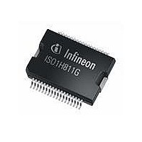
ISO1H811G Infineon Technologies, ISO1H811G Datasheet - Page 5

ISO1H811G
Manufacturer Part Number
ISO1H811G
Description
IC SWITCH HISIDE 8CH DSO-36
Manufacturer
Infineon Technologies
Type
High Sider
Series
ISOFACE™r
Datasheet
1.ISO1H811G.pdf
(20 pages)
Specifications of ISO1H811G
Package / Case
DSO-36
Input Type
Non-Inverting
Number Of Outputs
8
On-state Resistance
150 mOhm
Current - Output / Channel
700mA
Current - Peak Output
1.4A
Voltage - Supply
11 V ~ 35 V
Operating Temperature
-25°C ~ 125°C
Mounting Type
Surface Mount
Product
Driver ICs - Various
Propagation Delay Time
10 ns
Supply Voltage (max)
6.5 V
Supply Voltage (min)
- 0.5 V
Maximum Power Dissipation
3.3 W
Maximum Operating Temperature
Internally Limited
Mounting Style
SMD/SMT
Minimum Operating Temperature
- 25 C
Lead Free Status / RoHS Status
Lead free / RoHS Compliant
Lead Free Status / RoHS Status
Lead free / RoHS Compliant, Lead free / RoHS Compliant
Other names
SP000413798
Available stocks
Company
Part Number
Manufacturer
Quantity
Price
Part Number:
ISO1H811G
Manufacturer:
INFINEON/英飞凌
Quantity:
20 000
Company:
Part Number:
ISO1H811GAUMA1
Manufacturer:
TI
Quantity:
1 400
1.2
VCC (Positive 3.3/5V logic supply)
The VCC supplies the input interface that is
galvanically isolated from the output driver stage. The
input interface can be supplied with 3.3/5V.
DIS (Output disable)
The
immediately switched off by means of the low active pin
DIS that is an asynchronous signal. The input registers
are also reset by the DIS signal. The Output remains
switched off after low-high transition of DIS signal, till
new information is written into the input register.
Current Sink to GNDCC.
CS (Chip select)
The system microcontroller selects the ISO1H811G by
means of the low active pin CS to activate the parallel
interface. By connecting the CS pin and WR pin to
ground the parallel direct control is activated. Current
Source to VCC.
WR (Parallel write)
In parallel mode data at the input pins (D0 ... D7) are
latched by means of the rising edge of the low active
signal WR (write). Current Source to VCC.
D0 ... D7 (Data input bit0 ... bit7)
The present data can be latched on the rising edge of
the write signal WR. D0 ... D7 control the corresponding
output channels OUT0 ...OUT7. By connecting CS and
WR to ground, the signals at D0 ... D7 directly control
the outputs. Current Sink to GNDCC.
DIAG (Common diagnostic output for
overtemperature)
The low active DIAG signal contains the OR-wired
information of the separated overtemperature detection
units for each channel.The output pin DIAG provides an
open drain functionality. A current source is also
connected to the pin DIAG. In normal operation the
signal DIAG is high. When overtemperature or Vbb
below ON-Limit is detected the signal DIAG changes to
low.
GNDCC (Ground for VCC domain)
This pin acts as the ground reference for the input
interface that is supplied by VCC.
GNDbb (Output driver ground domain)
This pin acts as the ground reference for the output
Datasheet
high-side
Pin Functionality
outputs
OUT0...OUT7
can
be
5
driver that is supplied by Vbb.
OUT0 ... OUT7 (High side output channel 0 ... 7)
The output high side channels are internally connected
to Vbb and controlled by the corresponding data input
pins D0 ... D7 in parallel mode.
TAB (Vbb, Positive supply for output driver)
The heatslug is connected to the positive supply port of
the output interface.
Pin Configuration and Functionality
Version 2.1, 2009-05-28
ISOFACE
ISO1H811G
TM


