L6563STR STMicroelectronics, L6563STR Datasheet
L6563STR
Specifications of L6563STR
Available stocks


Related parts for L6563STR


L6563STR Summary of contents
Page 1
Features ■ Tracking boost function ■ Fast “bidirectional” input voltage feedforward 2 (1/V correction) ■ Interface for cascaded converter's PWM controller ■ Remote ON/OFF control ■ Accurate adjustable output overvoltage protection ■ Protection against feedback loop disconnection (latched shutdown) ■ ...
Page 2
Contents Contents 1 Description . . . . . . . . . . . . . . . . . . . . . . . . . . . . . . . . . . . . ...
Page 3
L6563S List of table Table 1. Absolute maximum ratings . . . . . . . . . . . . . . . . . . . . . . . . . . . . . . . ...
Page 4
List of figure List of figure Figure 1. Block diagram . . . . . . . . . . . . . . . . . . . . . . . . . . . . . . ...
Page 5
L6563S Figure 49. L6563S 100 W TM PFC demonstration board: compliance to EN61000-3-2 standard . . . 36 Figure 50. L6563S 100 W TM PFC demonstration board: compliance to JEITA-MITI standard . . . . . 36 Figure 51. L6563S ...
Page 6
Description 1 Description The L6563S is a current-mode PFC controller operating in transition mode (TM). Coming with the same pin-out as its predecessor L6563, it offers improved performance and additional functions. The highly linear multiplier, along with a special correction ...
Page 7
L6563S 2 Maximum ratings 2.1 Absolute maximum ratings Table 1. Absolute maximum ratings Symbol Vcc --- --- Analog inputs and outputs V PWM_STOP I PWM_STOP I ZCD VFF pin Other pins ...
Page 8
Pin connection 3 Pin connection Figure 2. Pin connection Table 3. Pin description n° Name Inverting input of the error amplifier. The information on the output voltage of the PFC pre- regulator is fed into the pin through a resistor ...
Page 9
L6563S Table 3. Pin description (continued) n° Name PFC pre-regulator output voltage monitoring/disable function. This pin senses the output voltage of the PFC pre-regulator through a resistor divider and is used for protection purposes. If the voltage on the pin ...
Page 10
Pin connection Figure 3. Typical system block diagram 10/43 Doc ID 16116 Rev 4 L6563S ...
Page 11
L6563S 4 Electrical characteristics T = -25 to 125 ° MΩ between pin VFF and GND; unless otherwise specified. FF Electrical characteristics Table 4. Symbol Parameter Supply voltage Vcc Operating range Vcc Turn-on threshold On ...
Page 12
Electrical characteristics Electrical characteristics (continued) Table 4. Symbol Parameter Gv Voltage gain GB Gain-bandwidth product Source current I COMP Sink current Upper clamp voltage V Burst-mode voltage COMP Lower clamp voltage Current sense comparator I Input bias current CS t ...
Page 13
L6563S Electrical characteristics (continued) Table 4. Symbol Parameter Triggering voltage V ZCDT (negative-going edge) I Input bias current ZCDb I Source current capability ZCDsrc I Sink current capability ZCDsnk Tracking boost function ΔV Dropout voltage V I Linear operation TBO ...
Page 14
Electrical characteristics Electrical characteristics (continued) Table 4. Symbol Parameter V Linear operation range VFF PWM_LATCH I Low level leakage current leak V High level H V High level H V High level H Gate driver V Output low voltage OL ...
Page 15
L6563S 5 Typical electrical performance Figure 4. IC consumption vs V 100 10 1 Co=1nF f =70kHz Tj = 25°C 0.1 0.01 0. 001 Vcc [V ] Figure 6. Vcc Zener voltage vs T ...
Page 16
Typical electrical performance Figure 8. Feedback reference vs T 2. 2. -50 - (C) Figure 10. UVLO saturation vs T 1 0.9 0.8 0.7 0.6 0.5 0.4 ...
Page 17
L6563S Figure 12. Inductor saturation threshold vs T 1.9 1.8 1.7 1.6 1.5 1.4 1.3 1.2 1.1 -50 - (C) Figure 14. ZCD sink/source capability vs T ...
Page 18
Typical electrical performance Figure 16. TBO clamp vs T 3.5 3.25 3 2.75 2.5 -50 - (C) Figure 18 current mismatch vs T INV TBO ...
Page 19
L6563S Figure 20. R discharge vs T -50 - (C) Figure 22 dropout vs T MULTpk VFF ...
Page 20
Typical electrical performance Figure 24. PFC_OK FFD threshold vs T 2 1.9 1.8 1.7 1.6 1.5 1.4 -50 - Tj(C) Figure 26. RUN threshold vs T 0 VCC = ...
Page 21
L6563S Figure 28. Multiplier characteristics @ 0.2 ...
Page 22
Typical electrical performance Figure 32. Gate drive output saturation vs T -50 - (C) Figure 34. Start-up timer period vs T 450 400 350 300 250 ...
Page 23
L6563S 6 Application information 6.1 Overvoltage protection Normally, the voltage control loop keeps the output voltage Vo of the PFC pre-regulator close to its nominal value, set by the ratio of the resistors R1 and R2 of the output divider. ...
Page 24
Application information 6.2 Feedback failure protection (FFP) The OVP function above described handles “normal” over voltage conditions, i.e. those resulting from an abrupt load/line change or occurring at start-up. In case the overvoltage is generated by a feedback disconnection, for ...
Page 25
L6563S Figure 36. Voltage feedforward: squarer-divider (1/V In this way a change of the line voltage will cause an inversely proportional change of the half sine amplitude at the output of the multiplier (if the line voltage doubles the amplitude ...
Page 26
Application information The twice-mains-frequency (2 peak amplitude that, with good approximation, is given by: where f is the line frequency. The amount of 3rd harmonic distortion introduced by this L ripple, related to the amplitude of its 2 Figure 37 ...
Page 27
L6563S 6.4 THD optimizer circuit The L6563S is provided with a special circuit that reduces the conduction dead-angle occurring to the AC input current near the zero-crossings of the line voltage (crossover distortion). In this way the THD (total harmonic ...
Page 28
Application information Figure 39. THD optimization: standard TM PFC controller (left side) and L6563S (right side) Rectified mains voltage Imains Input current Essentially, the circuit artificially increases the ON-time of the power switch with a positive offset added to ...
Page 29
L6563S V(TBO)/RT, that is internally 1:1 mirrored and sunk from pin INV (#1) input of the L6563S's error amplifier. In this way, when the mains voltage increases the voltage at TBO pin will increase as well and so will do ...
Page 30
Application information Figure 40. Tracking boost block Figure 41. Tracking output voltage vs Input voltage characteristic with TBO 6.6 Inductor saturation detection Boost inductor's hard saturation may be a fatal event for a PFC pre-regulator: the current up- slope becomes ...
Page 31
L6563S occasionally slightly saturate when the PFC stage is restarted because of a larger load demand. This happens when the restart occurs at an unfavorable line voltage phase, i.e. when the output voltage is significantly below the rectified peak voltage. ...
Page 32
Application information Figure 43. Interface circuits that let dc-dc converter's controller IC drive L6563S in burst mode The third communication line is the pin PWM_STOP (#9), which works in conjunction with the pin RUN (#10). The purpose of the PWM_STOP ...
Page 33
L6563S Figure 45. Interface circuits for power up sequencing when dc-dc has the SS function If this is not the case not possible to achieve a start-up delay long enough (because this prevents the dc-dc stage from ...
Page 34
Application information In table possible to find a summary of all of the above mentioned working conditions that cause the device to stop operating. Figure 47. Brownout protection (master PFC) Table 5. Summary of L6563S idle states ...
Page 35
L6563S 7 Application examples and ideas Figure 48. Demonstration board EVL6563S-100W, wide-range mains: electrical schematic Application examples and ideas Doc ID 16116 Rev 4 35/43 ...
Page 36
Application examples and ideas Figure 49. L6563S 100 W TM PFC demonstration board: compliance to EN61000-3-2 standard Meas ured value 1 0.1 0.01 0.001 0.0001 ...
Page 37
L6563S Figure 53. EVL6563S-250W TM PFC demonstration board: electrical schematic F1 F1 FUSE 4A FUSE 470N-X2 470N-X2 90-264Vac LH30-792Y3R0-01 LH30-792Y3R0- 2M2 2M2 R8 R8 PCB REV. 1 ...
Page 38
Application examples and ideas Figure 55. EVL6563S-ZRC200W 200W PFC pre-regulator with ripple-free input current: electrical schematic 330nF 330nF CX2 CX2 38/43 Doc ID 16116 Rev 4 L6563S ...
Page 39
L6563S 8 Package mechanical data In order to meet environmental requirements, ST offers these devices in different grades of ® ECOPACK packages, depending on their level of environmental compliance. ECOPACK specifications, grade definitions and product status are available at: www.st.com. ...
Page 40
Package mechanical data Figure 56. Package dimensions 40/43 Doc ID 16116 Rev 4 L6563S ...
Page 41
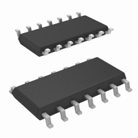
... L6563S 9 Ordering codes Table 7. Ordering information Order codes L6563S L6563STR Package SO14 Doc ID 16116 Rev 4 Ordering codes Packing Tube Tape and reel 41/43 ...
Page 42
Revision history 10 Revision history Table 8. Document revision history Date 12-Aug-2009 03-Sep-2009 29-Jan-2010 21-Dec-2010 42/43 Revision 1 Initial release. 2 Updated mechanical data. 3 Updated Table 4 on page Updated Figure 1 on page 4 page 8, Table 4 ...
Page 43
... L6563S Information in this document is provided solely in connection with ST products. STMicroelectronics NV and its subsidiaries (“ST”) reserve the right to make changes, corrections, modifications or improvements, to this document, and the products and services described herein at any time, without notice. All ST products are sold pursuant to ST’s terms and conditions of sale. ...