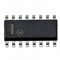
NCP1651DR2G ON Semiconductor, NCP1651DR2G Datasheet - Page 15

NCP1651DR2G
Manufacturer Part Number
NCP1651DR2G
Description
IC PFC CONTROLLER CCM/DCM 16SOIC
Manufacturer
ON Semiconductor
Datasheet
1.NCP1651DR2G.pdf
(32 pages)
Specifications of NCP1651DR2G
Mode
Continuous Conduction (CCM), Discontinuous Conduction (DCM)
Frequency - Switching
250kHz
Current - Startup
8.5mA
Voltage - Supply
10 V ~ 18 V
Operating Temperature
-40°C ~ 125°C
Mounting Type
Surface Mount
Package / Case
16-SOIC (3.9mm Width)
Switching Frequency
25 KHz to 250 KHz
Maximum Operating Temperature
+ 125 C
Mounting Style
SMD/SMT
Minimum Operating Temperature
- 40 C
Lead Free Status / RoHS Status
Lead free / RoHS Compliant
Other names
NCP1651DR2GOS
NCP1651DR2GOS
NCP1651DR2GOSTR
NCP1651DR2GOS
NCP1651DR2GOSTR
Available stocks
Company
Part Number
Manufacturer
Quantity
Price
Part Number:
NCP1651DR2G
Manufacturer:
ON/安森美
Quantity:
20 000
Results
converter operating in CCM has half the peak current and
one tenth the fundamental (100 kHz) harmonic current
compared to a flyback PFC converter operating in DCM.
The results are lower conduction losses in the MOSFET, and
secondary rectifying diode, and a smaller input EMI filter if
the designer needs to meet the requirements C.I.S.P.R.
conducted emission levels. On the down side to CCM
operation, the flyback transformer will be larger because of
the required higher primary inductance.
switching losses because the current falls to zero prior to the
next switching cycle, and smaller transformer size.
trade- -off study to determine which topology, Boost versus
Flyback, Continuous versus Discontinuous Mode of
operation will meet all the system performance
requirements. But the recent introduction of the NCP1651
allows the system designer one additional option.
converter, determining the transformer parameters (primary
inductance and turns ratio) involves several trade- -offs.
These include peak- -to- -average current ratio (higher
inductance or turns ratio result in lower peak current),
switching losses (higher turns ratio leads to higher peak
voltage and higher switching losses), CCM vs. DCM
operation (lower values of turns ratio or higher values of
inductance extend the CCM range) and range of duty cycles
over the operational line and load range. ON Semiconductor
has designed an Excel- -based spreadsheet to help design
with the NCP1651 and balance these trade- -offs. The design
aid is downloadable free- -of- -charge from our website
(www.onsemi.com).
requirements and the relative priority between factors such
as THD performance, cost, size and efficiency. The design
aid allows the designer to consider different scenarios and
settle on the best solution foe a given application. Following
guidelines will help in settling towards the most feasible
solution.
It is clear from the result of our analysis that a flyback PFC
The advantages to operating in DCM include lower
It will ultimately be up to the designer to perform a
For an average current mode flyback topology based PFC
The ideal solution depends on the specific application
1. Turns Ratio Limitations: While higher turns ratio
can limit the reflected primary voltage and current,
it is constrained by the inherent limitations of the
http://onsemi.com
15
PFC Operation
a small block of circuitry, which comprises the DC
regulation loop and the PFC circuit. These components are
shown in Figure 30.
rectified sinewave, the instantaneous input current and the
error signal at the FB/SD pin.
factor due to the control of the AC error amplifier. This
amplifier uses information from the AC input voltage and
the AC input current to control the power switch in a manner
that gives good DC regulation as well as excellent power
factor.
fullwave rectified sinewave. One of its inputs is connected
to a scaled down fullwave rectified sinewave, and the other
receives the error signal which has been converted to a
current. The error signal adjusts the level of the fullwave
rectified sinewave on the multiplier’s output without
distorting it. To accomplish this, it is necessary for the
bandwidth of the DC error amp to be less than twice the
lowest line frequency. Typically it is set at a factor of ten less
than the rectified frequency (e.g. for a 60 Hz input, the
bandwidth would be 12 Hz).
The basic PWM function of the NCP1651 is controlled by
There are three inputs to this loop. They are the fullwave
The input current is forced to maintain a near unity power
The reference multiplier sets a reference level for the input
2. CCM Operation: The NCP1651 is designed to
3. Following key governing equations have been
flyback topology. A turns ratio of higher than 20:1
will result in very high leakage inductance and
lead to high leakage spikes on the primary switch.
Thus, practical application of this approach is
restricted to output voltages 12 V and above.
operate in both CCM and DCM modes. However,
the CCM operation results in much better THD
than the DCM operation. Thus, it is recommended
that the circuit be designed to operate in CCM at
the specified test condition for harmonics
compliance (typically at 230 V, full load). Please
keep in mind that at or near zero crossing
(<10 deg angle), it is neither necessary nor feasible
to maintain CCM operation.
incorporated in the design aid:


