L9951 STMicroelectronics, L9951 Datasheet - Page 19
L9951
Manufacturer Part Number
L9951
Description
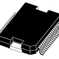
IC REAR DOOR ACT DVR POWERSO-36
Manufacturer
STMicroelectronics
Type
DC Motor Driverr
Datasheet
1.L9951XPTR.pdf
(36 pages)
Specifications of L9951
Applications
Automotive
Current - Supply
7mA
Voltage - Supply
7 V ~ 28 V
Operating Temperature
-40°C ~ 150°C
Mounting Type
Surface Mount
Package / Case
PowerSO-36 Exposed Bottom Pad
Operating Current
20mA
Operating Temperature Classification
Automotive
Motor Controller Type
DC Motor Driver
Package Type
PowerSO
Operating Supply Voltage (min)
7V
Operating Supply Voltage (max)
28V
Supply Current
20 mA
Mounting Style
SMD/SMT
Lead Free Status / RoHS Status
Lead free / RoHS Compliant
Available stocks
Company
Part Number
Manufacturer
Quantity
Price

Part Number:
L9951
Manufacturer:
ST
Quantity:
20 000
Part Number:
L9951XP
Manufacturer:
ST
Quantity:
20 000
Company:
Part Number:
L9951XPTR
Manufacturer:
st
Quantity:
6 966
Part Number:
L9951XPTR
Manufacturer:
ST
Quantity:
20 000


L9951 / L9951XP
3
3.1
3.2
3.3
3.4
Application information
Dual power supply: V
The power supply voltage V
charge-pump is used to drive the high side switches. The logic supply voltage V
(stabilized 5V) is used for the logic part and the SPI of the device. Due to the independent
logic supply voltage the control and status information will not be lost, if there are temporary
spikes or glitches on the power supply voltage. In case of power-on (V
under voltage to V
power-on-reset (POR).
If the voltage V
outputs are switched to tristate (high impedance) and the status registers are cleared.
Standby - mode
The standby mode of the L9951 is activated by switching the EN input do GND. All latched
data will be cleared and the inputs and outputs are switched to high impedance. In the
standby mode the current at V
If EN is switched to 5V the device will enter the active mode. In the active mode the charge-
pump and the supervisor functions are activated.
Inductive loads
Each half bridge is built by an internally connected high side and a low side power DMOS
transistor. Due to the built-in reverse diodes of the output transistors, inductive loads can be
driven at the outputs OUT1 to OUT3 without external free-wheeling diodes. The high side
drivers OUT4 to OUT5 are intended to drive resistive loads. Hence only a limited energy
(E<0.5mJ) can be dissipated by the internal ESD-diodes in freewheeling condition. For
inductive loads (L > 50µH) an external free-wheeling diode connected to GND and the
corresponding output is needed.
Diagnostic functions
All diagnostic functions (over/open-load, power supply over-/undervoltage, temperature
warning and thermal shutdown) are internally filtered and the condition has to be valid for at
least 32µs (open-load: 1ms, respectively) before the corresponding status bit in the status
registers will be set. The filters are used to improve the noise immunity of the device. Open-
load and temperature warning function are intended for information purpose and will not
change the state of the output drivers. On contrary, the over load and thermal shutdown
condition will disable the corresponding driver (over load) or all drivers (thermal shutdown),
respectively. Without setting the over-current recovery bit in the Input Data Register to logic
high, the microcontroller has to clear the over-current status bit to reactivate the
corresponding driver. Each driver has a corresponding over-current recovery bit. If this bit is
set, the device will automatically switch-on the outputs again after a short recovery time. The
duty cycle in over-current condition can be programmed by the SPI interface (12% or 25%).
With this feature the device can drive loads with start-up currents higher than the over-
current limits (e.g. inrush current of lamps, cold resistance of motors and heaters).
CC
POR OFF
decreases under the minimum threshold (V
= 4.0V, typical) the circuit is initialized by an internally generated
S
supplies the half bridges and the high side drivers. An internal
S
Doc ID 14173 Rev 8
(V
S
CC
and V
) is less than 3 µA (1µA) for CSN = high (DO in tristate).
CC
POR ON
Application information
=3.6V, typical), the
CC
increases from
CC
19/36
Related parts for L9951
Image
Part Number
Description
Manufacturer
Datasheet
Request
R

Part Number:
Description:
STMicroelectronics [RIPPLE-CARRY BINARY COUNTER/DIVIDERS]
Manufacturer:
STMicroelectronics
Datasheet:
Part Number:
Description:
STMicroelectronics [LIQUID-CRYSTAL DISPLAY DRIVERS]
Manufacturer:
STMicroelectronics
Datasheet:

Part Number:
Description:
BOARD EVAL FOR MEMS SENSORS
Manufacturer:
STMicroelectronics
Datasheet:
Part Number:
Description:
NPN TRANSISTOR POWER MODULE
Manufacturer:
STMicroelectronics
Datasheet:
Part Number:
Description:
TURBOSWITCH ULTRA-FAST HIGH VOLTAGE DIODE
Manufacturer:
STMicroelectronics
Datasheet:
Part Number:
Description:
Manufacturer:
STMicroelectronics
Datasheet:
Part Number:
Description:
DIODE / SCR MODULE
Manufacturer:
STMicroelectronics
Datasheet:
Part Number:
Description:
DIODE / SCR MODULE
Manufacturer:
STMicroelectronics
Datasheet:
Part Number:
Description:
Search -----> STE16N100
Manufacturer:
STMicroelectronics
Datasheet:
Part Number:
Description:
Search ---> STE53NA50
Manufacturer:
STMicroelectronics
Datasheet:
Part Number:
Description:
NPN Transistor Power Module
Manufacturer:
STMicroelectronics
Datasheet:
Part Number:
Description:
DIODE / SCR MODULE
Manufacturer:
STMicroelectronics
Datasheet: