LP3927ILQ-AZ/NOPB National Semiconductor, LP3927ILQ-AZ/NOPB Datasheet - Page 16
LP3927ILQ-AZ/NOPB
Manufacturer Part Number
LP3927ILQ-AZ/NOPB
Description
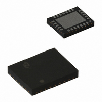
IC PWR MNGMNT CELL/PCS 28-LLP
Manufacturer
National Semiconductor
Datasheet
1.LP3927ILQX-AP.pdf
(17 pages)
Specifications of LP3927ILQ-AZ/NOPB
Applications
Handheld/Mobile Devices
Current - Supply
5µA
Voltage - Supply
3 V ~ 5.5 V
Operating Temperature
-40°C ~ 85°C
Mounting Type
Surface Mount
Package / Case
28-LLP
Lead Free Status / RoHS Status
Lead free / RoHS Compliant
Other names
LP3927ILQ-AZ


www.national.com
Application Hints
surement, junction to ambient thermal resistance (θ
be improved by as much as two times if a LLP is soldered on
the board with thermal land and thermal vias than if not.
Consider the following equation:
Where P is the power dissipated, T
temperature of the die, T
θ
at 150˚C.
According to the above equation, in the case where the
LP3927 is dissipating 3W of power, T
when T
equation. In order to operate at a higher ambient tempera-
ture, power dissipation has to be reduced. A curve of maxi-
mum power dissipation vs ambient temperature is provided
below.
JA
is the thermal resistance of the package. T
Power Dissipation vs Ambient Temperature
J
of 125˚C and θ
(θ
JA
A
=30.8˚C/W)
JA
is the ambient temperature, and
of 30.8˚C/W are used in the
(Continued)
J
is the maximum junction
A
is limited to 32.6˚C
20037915
J
is specified
JA
) can
16
LAYOUT CONSIDERATION
The LP3927 has an exposed die attach pad located at the
bottom center of the LLP package. It is imperative to create
a thermal land on the PCB board when designing a PCB
layout for the LLP package. The thermal land helps to con-
duct heat away from the die, and the land should be the
same dimension as the exposed pad on the bottom of the
LLP (1:1 ratio). The land should be on both the top and the
bottom layer of the PCB board. In addition, thermal vias
should be added inside the thermal land to conduct more
heat away from the surface of the PCB to the ground plane.
Typical pitch and outer diameter for these thermal vias are
1.27 mm and 0.33 mm respectively. Typical copper via barrel
plating is 1 oz. although thicker copper may be used to
improve thermal performance. The LP3927 bottom pad is
connected to ground. Therefore, the thermal land and vias
on the PCB board need to be connected to ground.
For more information on board layout techniques, refer to
Application Note 1187 “Leadless Leadframe Package
(LLP).” The application note also discusses package han-
dling, solder stencil, and assembly process.
Related parts for LP3927ILQ-AZ/NOPB
Image
Part Number
Description
Manufacturer
Datasheet
Request
R

Part Number:
Description:
IC PWR MANAGEMENT CELL/PCS 28LLP
Manufacturer:
National Semiconductor
Datasheet:
Part Number:
Description:
IC PWR MANAGEMENT CELL/PCS 28LLP
Manufacturer:
National Semiconductor
Datasheet:

Part Number:
Description:
IC PWR MNGMNT CELL/PCS 28-LLP
Manufacturer:
National Semiconductor
Datasheet:

Part Number:
Description:
IC,Power Control/Management,LLCC,28PIN,PLASTIC
Manufacturer:
National Semiconductor
Part Number:
Description:
Cellular/PCS System Power Management IC
Manufacturer:
National Semiconductor
Datasheet:

Part Number:
Description:
Cellular/PCS System Power Management IC
Manufacturer:
NSC [National Semiconductor]
Datasheet:
Part Number:
Description:
National Semiconductor [8-Bit D/A Converter]
Manufacturer:
National Semiconductor
Datasheet:
Part Number:
Description:
National Semiconductor [Media Coprocessor]
Manufacturer:
National Semiconductor
Datasheet:
Part Number:
Description:
Digitally Controlled Tone and Volume Circuit with Stereo Audio Power Amplifier, Microphone Preamp Stage and National 3D Sound
Manufacturer:
National Semiconductor
Datasheet:
Part Number:
Description:
Digitally Controlled Tone and Volume Circuit with Stereo Audio Power Amplifier, Microphone Preamp Stage and National 3D Sound
Manufacturer:
National Semiconductor
Datasheet:
Part Number:
Description:
AC97 Rev 2 Codec with Sample Rate Conversion and National 3D Sound
Manufacturer:
National Semiconductor
Part Number:
Description:
Manufacturer:
National Semiconductor
Datasheet:
Part Number:
Description:
Manufacturer:
National Semiconductor
Datasheet:
Part Number:
Description:
General Purpose, Low Voltage, Low Power, Rail-to-Rail Output Operational Amplifiers
Manufacturer:
National Semiconductor
Datasheet: