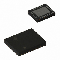
LP3927ILQ-AZ/NOPB National Semiconductor, LP3927ILQ-AZ/NOPB Datasheet - Page 8

LP3927ILQ-AZ/NOPB
Manufacturer Part Number
LP3927ILQ-AZ/NOPB
Description
IC PWR MNGMNT CELL/PCS 28-LLP
Manufacturer
National Semiconductor
Datasheet
1.LP3927ILQX-AP.pdf
(17 pages)
Specifications of LP3927ILQ-AZ/NOPB
Applications
Handheld/Mobile Devices
Current - Supply
5µA
Voltage - Supply
3 V ~ 5.5 V
Operating Temperature
-40°C ~ 85°C
Mounting Type
Surface Mount
Package / Case
28-LLP
Lead Free Status / RoHS Status
Lead free / RoHS Compliant
Other names
LP3927ILQ-AZ
www.national.com
C
V
I
SR
GBW
S
Symbol
Electrical Characteristics, Operational Amplifier
OUT
Unless otherwise noted, V
appearing in normal type apply for T
range for operation, −40˚C to +85˚C. (Note 7)
IN
Note 1: Absolute Maximum Ratings are limits beyond which damage to the device may occur. Operating Ratings are conditions under which operation of the device
is guaranteed. Operating Ratings do not imply guaranteed performance limits. For guaranteed performance limits and associated test conditions, see the Electrical
Characteristics tables.
Note 2: All voltages are with respect to the potential at the GND pin.
Note 3: The Absolute Maximum power dissipation depends on the ambient temperature and can be calculated using the formula
where T
Absolute Maximum Ratings results from substituting the Absolute Maximum junction temperature, 150˚C, for T
be dissipated safely at ambient temperatures below 70˚C. Less power can be dissipated safely at ambient temperatures above 70˚C. The Absolute Maximum power
dissipation can be increased by 32.5 mW for each degree below 70˚C, and it must be derated by 32.5 mW for each degree above 70˚C.
Note 4: The human-body model is used. The human-body model is 100 pF discharged through 1.5 kΩ.
Note 5: This figure is taken from a thermal modeling result. The test board is a 4 layer FR-4 board measuring 101mm x 101mm x 1.6mm with a 3 x 3 array of thermal
vias. The ground plane on the board is 50mm x 50mm. Ambient temperature in simulation is 22˚C, still air. Power dissipation is 1W.
Note 6: Like the Absolute Maximum power dissipation, the maximum power dissipation for operation depends on the ambient temperature. The 1.78W rating
appearing under Operating Ratings results from substituting the maximum junction temperature for operation, 125˚C, for T
(1) above. More power can be dissipated at ambient temperatures below 70˚C. Less power can be dissipated at ambient temperatures above 70˚C. The maximum
power dissipation for operation can be increased by 32.5 mW for each degree below 70˚C, and it must be derated by 32.5 mW for each degree above 70˚C.
Note 7: All limits guaranteed at room temperature (standard typeface) and at temperature extremes (bold typeface). All room temperature limits are 100%
production tested or guaranteed through statistical analysis. All limits at temperature extremes are guaranteed via correlation using standard Statistical Quality
Control (SQC) methods.
Note 8: The target output voltage, which is labeled V
Note 9: Dropout voltage is the input-to-output voltage difference at which the output voltage is 100 mV below its nominal value. This specification does not apply
in cases it implies operation with an input voltage below the 2.5V minimum appearing under Operating Ratings. For example, this specification does not apply for
devices having 1.5V outputs because the specification would imply operation with an input voltage at or about 1.5V.
Note 10: Pulsing the load of LDO X from 100µA to Imax and measuring its effects at the output of LDO Y. LDO Y enabled but under no load.
Note 11: The error flags are internal to the chip. There is no external access to the signals. LDO1 error flag and the LDO2 error flag will go HIGH when the respective
LDO reaches its V
Note 12: The t
its error flag going LOW. Same delays apply to LDO2 and its error flag.
Note 13: Refer to Timing Diagram.
Note 14: The delay between LDO2 error flag HIGH and RST signal HIGH in the power up sequence. In the power down sequence, it is the delay between RST
signal LOW and LDO2 disabled.
Note 15: The delay between LDO1 error flag HIGH and LDO2 enable in power up sequence. In the power down sequence, it is the delay between LDO2 error flag
LOW and LDO1 disable. For the optional LDO delay, please contact the factory for availability.
Note 16: Time between RST high and PS_HOLD going high.
J
is the junction temperature, T
Common-Mode Input Capacitor
Output Swing
Supply Current
Slew Rate
Gain-Bandwidth Product
DELAY-H
Th-H
value. The error flags will go LOW when the respective LDO reaches its V
is the delay between LDO1 reaching its V
OP_AMP_VDD
Parameter
A
is the ambient temperature, and θ
J
= 25˚C. Limits appearing in boldface type apply over the entire junction temperature
= 3.3V, V
OUT(target)
CM
, is the desired or ideal output voltage.
Th-H
= V
P = (T
and its error flag going HIGH. The t
OUT
R
V
OP_AMP_VDD
= V
LOAD
J
JA
− T
8
is the junction-to-ambient thermal resistance. The 2.6W rating appearing under
OP_AMP_VDD
= 2 kΩ
A
Conditions
)/θ
JA
,
= 3.0V
/2 and R
Th-L
value.
DELAY-L
(Continued)
LOAD
J
, 70˚C for T
is the delay between LDO1 reaching its V
Typical
>
0.5
0.7
0.6
1 MΩ. Typical values and limits
3
A
J
, and 30.8˚C/W for θ
, 70˚C for T
Min
3.1
A
, and 30.8˚C/W for θ
Limit
Max
JA
0.5
1.4
. More power can
Th-L
Units
MHz
V/µs
JA
mA
pF
V
and
into
(1)


